Chapter 14: DDR3 initialization with MMDC
A store to OCRAM needs no memory-device initialization. The same store to
0x80000000 depends on an external chip, its power and clock, controller
timings, and the board’s routing. A correct address is only the beginning.
This chapter traces those dependencies through a board-specific initialization record and a small destructive-test example. The supplied core schematic shows a single x16 Nanya NT5CC256M16EP-EK on CS0, nominally 512 MiB. That device is the record’s starting point, not confirmation of the part fitted to an uninspected board.
Execution boundary: this chapter does not contain a qualified DDR initialization table. Obtain the exact part data sheet, board-matched BSP initialization, and i.MX6ULL-compatible NXP tools before attempting bring-up. Do not substitute illustrative timings or calibration values. If DDR is already initialized by a DCD/loader, do not reinitialize it under running code. You may study the sequence and use a verified loader configuration instead.
14.1 This chapter takes time
Keep the loader, UART diagnostics, constants, stack, and exception vectors in OCRAM while DDR is uncertain. A failed DDR read may hang rather than return a conveniently printable error. Print a checkpoint before each new phase; a last message can narrow the failing step.
Retain Chapter 10’s map and assertions: ROM-active loaded bytes must end
at or below 0x00918000; post-handoff owned stack space may extend up to
0x00920000 only when it no longer overlaps ROM use. Include every added
table and embedded payload in the load-size check.
MMU and D/L2 cache state must be established before destructive memory tests. Do not infer all caches are off from reset: RM section 8.4.4 describes ROM use of I-cache and disabling D/L2/MMU following authentication, not an unconditional I-cache-off handoff.
14.1a RAM/ROM/SRAM/SDRAM/DDR, the lineage
The useful distinction is whether software must keep the memory alive:
SRAM retains data while powered without DRAM-style refresh. OCRAM and CPU caches use SRAM; cost and area limit their capacity.
DRAM stores charge and needs refresh. SDRAM synchronizes commands to a clock; DDR is also synchronous DRAM.
DDR transfers data on both clock edges. DDR2/DDR3 increase prefetch depth and change electrical/protocol requirements.
DDR3 normally uses 1.5 V; DDR3L supports the low-voltage 1.35 V operating specification. Confirm the fitted part and actual rail.
LPDDR2 is a different supported protocol. LPDDR3, DDR4, and DDR5 are not supported by this i.MX6ULL controller configuration.
MMDC supports DDR3/DDR3L x16 and LPDDR2 x16, up to 400 MHz DDR CK
(RM 35.1). A 396 MHz CK transfers at 792 MT/s, not 396 MT/s:
396 million * 2 edges * 2 bytes = 1.584 GB/s theoretical data-bus peak.
Command overhead, refresh, and access patterns reduce usable bandwidth.
CK is not the DRAM cell-array clock.
14.2 DDR3, enough detail for bring-up
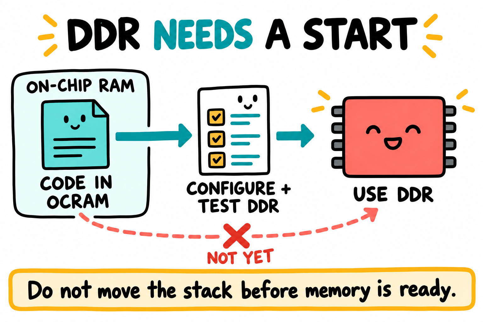
Keep the code and stack in known memory while investigating the new memory. The arrows show prerequisites, not an automatic copy operation. The DDR icon is generic. The fitted device and its required settings come from the board record.
The controller activates a row in one of eight banks, reads or writes columns in that open row, then precharges it before a different activation. Refresh commands restore charge across the array over a refresh window; one command does not refresh every row at once.
Symbol |
Requirement to find in the exact part data sheet |
|---|---|
|
Activate-to-read/write delay |
|
Precharge-to-activate delay |
|
Minimum row-active time |
|
Minimum row-cycle time |
|
Refresh command busy time, dependent on density |
|
Write recovery; also encoded in MR0 |
|
Four-activate window |
|
Permitted CAS latency and minimum access time at chosen CK |
|
Permitted CAS write latency at chosen CK; not universally CL-2 |
|
Refresh interval, including temperature-dependent requirements |
For a minimum in nanoseconds, start with
cycles = ceil(t_min_ns / tCK_ns), then apply minimum-cycle requirements
and the particular MMDC field encoding. Not every field is simply N-1.
For example, a hypothetical 15 ns minimum at 396 MHz needs six CK cycles. This is arithmetic, not a Nanya timing recommendation. A speed-bin label such as DDR3-1600 describes operation at 1600 MT/s (800 MHz CK); its latency numbers cannot be copied unchanged into a 396 MHz setup.
A timing record connects the data-sheet page, minimum ns, minimum cycles, chosen cycles, MMDC field and encoded value. A separate entry for the matching DRAM mode-register field exposes a controller/DRAM latency mismatch before the first access.
The supplied schematic names NT5CC256M16EP-EK. Obtain its manufacturer data sheet and confirm density, row/column geometry, speed suffix, temperature range, and low-frequency limits. A replacement device needs a fresh timing record, even when the pinout matches.
14.3 Two chips, one bus, channels, ranks, banks
A channel is a controller data interface. A rank is the set of devices selected together by one chip-select. Banks are internal arrays within a DRAM device.
Two x8 devices can form a x16 rank, but the supplied core schematic instead shows one x16 device on CS0. Both byte lanes come from that chip.
256 M locations * 16 bits = 4096 Mbits = 512 MiB
one x16 device, one rank, eight internal banks
For a candidate 15-row-bit, 10-column-bit, eight-bank x16 geometry:
2^15 * 2^10 * 8 * 2 bytes = 512 MiB. Check those counts in the exact
data sheet before encoding MDCTL and MDASP. A 14-row-bit version would
have half that capacity. A low-address test cannot distinguish them.
14.4 The MMDC register groups
MMDC base is 0x021B0000; its register descriptions are in RM Chapter 35.
Register/group |
Offset |
Responsibility |
|---|---|---|
MDCTL |
|
Geometry, bus width, chip-select enable |
MDPDC |
|
Power-down configuration |
MDOTC |
|
ODT timing |
MDCFG0 |
|
Includes tRFC, tXS, tXP, tXPDLL, tFAW, tCL |
MDCFG1 |
|
Includes tRCD, tRP, tRC, tRAS, tWR, tMRD, tCWL |
MDCFG2 |
|
Includes tDLLK, tRTP, tWTR, tRRD |
MDMISC |
|
Memory type and controller options |
MDSCR |
|
Configuration request/acknowledge and commands |
MDREF |
|
Refresh configuration |
MDRWD |
|
Read/write turnaround |
MDOR |
|
Reset/CKE wait timing |
MDASP |
|
Chip-select address-space partition |
MAARCR |
|
AXI reordering |
MAPSR |
|
Power saving/status |
MPZQHWCTRL |
|
PHY ZQ calibration |
MPWLGCR |
|
Write-leveling control |
MPWLDECTRL0 |
|
Write-leveling delays for byte lanes 0 and 1 |
MPDGCTRL0 |
|
Read DQS gating for the active lanes |
MPRDDLCTL |
|
Per-byte read delay |
MPWRDLCTL |
|
Per-byte write delay |
MPRDDQBY0DL..1DL |
|
Active byte-lane read DQ bit-delay controls |
MPMUR0 |
|
PHY measure-unit control/status |
The register map contains descriptions inherited from wider MMDC variants. Mark the two active byte lanes before following those descriptions.
MDSCR.CON_REQ blocks new AXI accesses and drains outstanding work. Poll CON_ACK before permitted configuration/commands, then clear CON_REQ after completion (RM 35.12.8). Command fields in MDSCR issue the DRAM commands; ordinary memory traffic waits while configuration is in progress. Polls need bounded failure handling that remains entirely outside DDR.
14.5 IOMUX before MMDC
DDR pads need the correct electrical configuration before command traffic. The dedicated DDR pad/group registers are in IOMUXC (RM Chapter 32). They select the memory interface’s electrical behavior, separately from the familiar GPIO alternate-function setup.
Record exact addresses and decoded fields for clock, address/control, DQS, DQ byte groups, CKE, ODT, reset, DDR type, and calibration reference settings from the board-matched configuration. Check reserved bits and the actual 1.35 V rail. Keep addresses and decoded fields together so each write can be checked against its register description.
Drive strength, slew, and termination interact with trace impedance and loading. Too much or too little drive can reduce the signal margin. A memtest mismatch is a starting point for diagnosis; waveform and margin measurements answer the electrical questions the schematic leaves open.
14.6 The JEDEC DDR3 initialization sequence
The part data sheet and MMDC procedure together define the actual sequence. For the DDR3 power-up outline:
Establish supplies as specified and hold RESET# low for the required power-up interval (at least 200 us for the usual DDR3 sequence).
Release RESET# while keeping CKE low for the required interval (usually at least 500 us after RESET# rises). Establish a valid clock for the specified time before CKE rises.
Assert CKE high, issue NOP/deselect, and wait tXPR before MRS.
Load MR2, MR3, MR1, then MR0 with DLL reset, observing tMRD and the final tMOD requirement.
Issue ZQCL and observe the specified ZQ initialization and DLL-lock waits before normal traffic.
Complete the controller/PHY calibration flow, restore operating modes and refresh, and release configuration request.
Follow the CKE rising edge closely: the reset-to-CKE wait happens before it, and tXPR happens afterward. MMDC MDOR and command sequencing implement parts of the procedure; verify their clock basis and encodings. Micron’s DDR3 FAQ also explains reset and ZQ behavior; it is background, not the fitted Nanya part’s timing authority.
Mode Register encodings (relevant fields)
Register |
Fields to decode from the fitted part’s data sheet |
|---|---|
MR0 |
BL at A1:A0; split CL field at A6:A4 and A2; DLL reset at A8; discrete tWR encoding at A11:A9 |
MR1 |
DLL disable at A0; output impedance at A5/A1; RTT_NOM at A9/A6/A2; write leveling at A7 |
MR2 |
CWL at A5:A3; RTT_WR at A10:A9; refresh-related options |
MR3 |
MPR/operating options required during calibration and normal use |
Choose supported CL/CWL values for the actual CK, not the maximum-speed bin. Compute DRAM MR values separately from MMDC timing encodings. Then encode the MR address and bank selection into MDSCR as documented. A bare MR value is not an entire MDSCR command.
Each MR’s source, chosen cycles and encoding belong to that same timing record.
14.7 Preparing the board-specific initialization
The timing record, pad configuration and calibration results together define the board’s initialization contract. The following outline names the phases that a board-owned implementation must supply:
Verified board-specific initialization:
  establish approved clock/voltage state and MMDC root
  configure exact DDR pads and groups
  enter/confirm MMDC configuration state
  program geometry, partition, timing, reset waits, ODT and PHY controls
  perform reset/CKE/MRS/ZQ sequence with required waits
  apply qualified calibration or run the complete calibration procedure
  restore refresh and normal operating options
  release configuration request; confirm completion
  test only an explicitly reserved, destructive scratch range
Start from the matching board BSP and NXP RPA, then check the fitted part and silicon errata. Keep the generated initialization, timing record, tool version, and calibration log together: they describe one configuration.
The test below is compilable. It requires already initialized DDR, an aligned, exclusively reserved range, MMU-off access with D-cache/L2 disabled under the startup policy, and all code/data/stacks in OCRAM. It overwrites every word twice. Volatile forces accesses in C; it does not bypass a cache.
ddr.h:
#ifndef DDR_H
#define DDR_H
#include <stdint.h>
int ddr_init(void); /* board-owned implementation; 0 = completed */
uint32_t ddr_test_words(volatile uint32_t *base, uint32_t words);
#endif
ddr-test.c (there is deliberately no generic ddr_init() definition):
#include "ddr.h"

uint32_t ddr_test_words(volatile uint32_t *base, uint32_t words)
{
    uint32_t errors = 0;
    for (uint32_t pass = 0; pass < 2; pass++) {
        uint32_t mask = pass ? 0x5A5A5A5Au : 0xA5A5A5A5u;
        for (uint32_t i = 0; i < words; i++) base[i] = i ^ mask;
        __asm__ volatile ("dsb sy" ::: "memory");
        for (uint32_t i = 0; i < words; i++)
            if (base[i] != (i ^ mask)) errors++;
    }
    return errors;
}
Limit the range so the pointer arithmetic is valid and the two-pass error count cannot overflow. The caller supplies the capacity and reserved-region checks. Zero errors mean this range passed these patterns on this run; wider coverage comes in section 14.11.
14.8 Calibration: write leveling, DQS gating, read/write delay
Calibration asks where to sample or drive data within a clock period:
Write leveling aligns write DQS with CK at the memory.
DQS gating finds the read-response strobe window.
Read/write delay calibration positions sampling/driving within the data window. The main delay registers operate per byte; separate DQ registers provide bit adjustments.
The hardware calibration procedure controls memory mode, configuration state, refresh, starting delays, completion polls, error checks, and restoration. Follow RM 35.11 and the tool’s matching user guide in order.
Recording the active-lane delays
On the i.MX6ULL x16 interface, MPWLDECTRL0 covers both active byte lanes. The corresponding registers with suffix 1 describe additional lanes in wider layouts. Keep that distinction beside the tool’s output:
Register |
Address |
Lane meaning |
|---|---|---|
MPWLDECTRL0 |
|
Write leveling, bytes 0 and 1 |
MPWLDECTRL1 |
|
Wider-layout bytes 2 and 3, not active x16 bytes |
MPDGCTRL0 |
|
DQS gating for active x16 lanes |
MPDGCTRL1 |
|
Wider-layout additional lanes |
MPRDDLCTL |
|
Read delay; use active byte fields |
MPWRDLCTL |
|
Write delay; use active byte fields |
Record the active-lane results with board revision, part marking, CK, voltage, temperature, tool version, and test settings. Use the matching i.MX6ULL procedure to decide which fields belong in the initialization.
Qualifying supported operating points
Qualify the chosen configuration at supported operating points across the specified voltage/temperature envelope, using appropriate equipment. For each point, record test coverage, duration, errors, and calibration margin. Stay within both the SoC and DRAM ratings; an overclock result cannot replace this qualification.
Review errata ERR005778 before DDR operation below 100 MHz (measure-unit workaround must execute outside DDR). ERR009596 requires MAARCR’s ARCR_GUARD bits to remain zero. Include those requirements in the same initialization record.
14.9 Calling from main() and the OCRAM → DRAM jump
Integrate this main-body fragment with the board-owned ddr_init(),
working UART/printf, Chapter 10 startup, and the test module. If a DCD/loader
already initialized DDR, retain that state and skip the initialization call.
/* In main(), while everything still lives in OCRAM: */
printf("Starting board DDR initialization\r\n");
if (ddr_init() != 0) {
    printf("DDR initialization did not complete\r\n");
    for (;;) {}
}
/* Example only: reserve 0x81000000..0x813FFFFF before using it. */
uint32_t errors = ddr_test_words((volatile uint32_t *)0x81000000u,
                                4u * 1024u * 1024u / 4u);
printf("DDR scratch test: %u mismatches\r\n", errors);
if (errors) for (;;) {}
That scratch span is 16 MiB above the base. Confirm it exists and reserve it in the memory map; it stays clear of the separate payload proposed below. Report the tested span and mismatch count rather than total-capacity success.
If a checkpoint disappears, investigate power/reset, CK, pads, geometry, timings, commands, refresh, and calibration. There is no evidence-based ranking of those causes in this chapter.
14.10 Copying ourselves to DRAM
Copying a fixed-address executable to a new base does not relocate it.
Literal addresses, global references, pointers, and vector entries still
refer to the old link addresses. A zero-initialized static flag usually
belongs to BSS, which is not stored in the raw payload. Printing &main
also prints a link-time address, not a measurement of the current PC.
A simpler design uses an OCRAM loader plus a separately linked DRAM payload. Each image has its own link addresses and startup. Their ownership boundary is explicit:
The example payload is linked at
0x80100000, with vectors first andENTRY(_vectors)as in Chapter 10. Its first ARM instruction branches to its own startup.Payload startup masks interrupts, initializes its own SVC/IRQ stacks and data/BSS, installs VBAR with the Chapter 15 policy and enters its own main. It must not reinitialize DDR.
The loader holds the raw payload in its read-only section, bounded by start/end symbols. Those bytes count toward the ROM-active OCRAM load bound, which may exclude a larger two-image bundle.
The loader tests an unrelated scratch range and copies exactly the payload file length into its linked destination. Both loader and payload regions remain excluded from subsequent destructive tests.
The handoff synchronizes the new instruction bytes before branching to the payload entry.
Embedding assembly fragment in a loader source file:
    .section .rodata.dram_payload, "a"
    .balign 4
    .global _payload_start, _payload_end
_payload_start:
    .incbin "dram-payload.bin"
_payload_end:
Copy C fragment; include stdint.h. Its symbols require the assembly
and linker integration above:
extern const unsigned char _payload_start[], _payload_end[];
extern void enter_dram_payload(uint32_t entry) __attribute__((noreturn));

void copy_and_enter_payload(void)
{
    uintptr_t bytes = (uintptr_t)_payload_end - (uintptr_t)_payload_start;
    volatile unsigned char *dst = (volatile unsigned char *)0x80100000u;
    /* Verify bytes and destination bounds against the payload map first. */
    for (uintptr_t i = 0; i < bytes; i++) dst[i] = _payload_start[i];
    enter_dram_payload(0x80100000u);
}
enter-dram.S, callable from that fragment under the explicit
MMU-off, D/L2-disabled, privileged SVC, ARM-state policy:
    .syntax unified
    .cpu cortex-a7
    .arm
    .text
    .global enter_dram_payload
    .type enter_dram_payload, %function
enter_dram_payload:
    cpsid if
    dsb sy
    mov r1, #0
    mcr p15, 0, r1, c7, c5, 0   @ invalidate I-cache to PoU
    mcr p15, 0, r1, c7, c5, 6   @ invalidate branch predictor
    dsb sy
    isb
    bx r0
    .size enter_dram_payload, . - enter_dram_payload
I-cache may still be enabled from ROM; synchronization is therefore explicit. If D-cache/L2 is enabled, this stub is insufficient: dirty destination data needs the correct clean-to-PoU/coherency procedure first. Do not add a casual cache-disable instruction and discard dirty data.
Use the payload map/disassembly and, when available, a debugger’s current PC to check execution in DRAM. Its stack, globals, and VBAR need separate checks. The later IRQ/timer examples can stay in OCRAM. Their mechanisms do not depend on relocating this payload or completing DDR qualification.
14.11 Sanity tests beyond the basic memtest
All tests are destructive. Keep the tester outside the tested range and disable other masters that might use it.
Walking ones / zeros
A walking-bit test writes each 1u << bit and its complement to a reserved
word, then compares the readback. It checks data-bit behavior at that
location, not every cell or address line. All-zero/all-one and alternating
patterns at multiple locations extend the pattern coverage.
Address-as-data
An address-as-data test writes distinct address-derived patterns across a reserved span before reading any back. A dedicated power-of-two address-alias test addresses a different coverage gap: a 4 MiB sweep cannot find every high address bit or a wrongly configured 256/512 MiB boundary.
Long memtest
A wider test uses multiple patterns and retention intervals within the available verified capacity, excluding loader, stacks, vectors, logs, payload and tool working areas. A tester running in DRAM cannot overwrite “all 512 MiB” safely. Its result is meaningful only with the range, duration, conditions and first failing address/value.
Linux memtester later tests memory allocated to a user process; it is not
a bare-metal program or a proof that every physical byte was tested.
14.12 Why the DCD is the elegant alternative
A DCD lets the ROM prepare DDR before loading a payload into it. Chapter 7 describes its write, check/poll, and NOP commands, format limits, and register-validation constraints. General branching and calibration algorithms require executable initialization code.
A validated DCD carries a fixed board configuration. An SPL can instead
execute richer initialization code. Choose the boot design first, then
express the board’s initialization in the form that design supports.
Chapter 11’s python3 mkimx.py tool is deliberately OCRAM-only and unsigned;
it does not build a DDR image or accept a DCD. The two-image design above
still wraps an OCRAM loader. For a ROM-loaded DDR image, follow the actual
Chapter 19 image/build route with a qualified DCD-capable configuration.
14.13 NXP’s DDR Stress Tool
Use NXP’s i.MX 6/7 DDR Stress Test Tool and the matching i.MX6UL/ULL/ULZ Register Programming Aid (RPA). Select the package by its supported SoCs; similarly named tools for i.MX8M serve a different controller.
The RPA derives an initialization script from the selected part geometry, timings, clock, and board configuration. The stress tool loads a helper, runs calibration/testing, and reports results. Supply the RPA-derived starting configuration before asking the tool to find delay margins. NXP’s tool release page identifies the supported SoCs and separate roles of the two tools.
Before a hardware session, read the matching package guide, check board power/USB/reset prerequisites from Chapter 8, and verify the selected SoC. Archive inputs and results. This chapter records no tool run or board test.
14.14 Key Notes
DDR availability depends on a matched clock, geometry, electrical setup, timing/command sequence, refresh and calibration. A valid address or a copied delay table establishes none of that configuration by itself.
MMDC fields and DRAM mode registers encode the same latency choices differently. Minimum nanoseconds, minimum CK cycles and field encodings must agree for the fitted part at the selected operating point.
Configuration request/acknowledge separates setup from normal AXI traffic. Failure handling must stay in OCRAM, because uncertain DDR cannot safely hold diagnostics, stacks or the recovery path.
Destructive tests require exclusive scratch ownership and a known cache state. A successful low-address sweep does not establish full capacity, high-address non-aliasing or voltage/temperature margin.
Calibration positions the active byte lanes within the data window. Its results belong to a particular board, DRAM part, clock and set of conditions, not to every board sharing the SoC.
A separately linked DRAM payload keeps loading distinct from relocation. It owns its startup, stack, globals and vectors, while the OCRAM loader owns placement and instruction synchronization. IRQ/timer examples need not move.
This chapter supplies no qualified DDR initialization table or board result. Temperature/voltage qualification requires controlled equipment within ratings. Do not use a hairdryer, hot-air station or DDR overclock as a stress experiment.
14.15 Pitfalls
Copied constants without provenance. Calibration is not a complete clock/pad/timing/refresh configuration.
Wrong capacity. A small test may pass while high addresses alias.
Mismatched CL/CWL. Controller and DRAM have different encodings but must agree on the chosen latencies.
Live MMDC reclocking. Timings are encoded for a particular CK.
Leaving CON_REQ asserted. Normal AXI traffic remains blocked.
Cache-only success. Volatile is not uncached memory.
Naive copy-and-call relocation. Link-time addresses do not move.
Blind retries. Follow the board’s approved reset/power sequence, including source/back-power checks; an arbitrary five-second wait is not proof of a clean reset.
14.16 Going deeper
The exact fitted DRAM manufacturer’s data sheet, including operating ranges, low-frequency limits, reset/MRS/ZQ timings, and MR encodings.
IMX6ULLRM Chapter 35, especially 35.11 and 35.12; Chapter 18 for clocks and Chapter 32 for pads.
i.MX6ULL errata, ERR005778 and ERR009596.
NXP i.MX 6/7 DDR tools, matching RPA and packaged stress-tool user guide.
AN4467, i.MX 6 Series DDR Calibration: background on the procedures; check applicability alongside the matching device/tool guide.
Board-matched BSP DCD/SPL: trace each value back to a worksheet or measured result rather than copying a different evaluation board’s memory table.
Next chapter: Chapter 15: Exceptions and the GIC. We can build the IRQ path in OCRAM with a known stack and vector table, independently of the optional DRAM payload.