Chapter 18: Optional bare-metal peripherals¶
A flash can receive four perfectly timed bytes and still ignore the command. If chip-select rises between the command and its reply, the flash sees separate transactions. A framebuffer can contain the right pixels while the LCD reads an older copy from DRAM. Neither problem is solved by finding another register address.
This chapter follows those boundaries: the whole bus transaction, then the whole buffer handoff. The controller logic will feel familiar from MCU work; the clock routes, pad inputs and cache ownership need a closer look.
We will trace an I2C single-byte random read, a SPI JEDEC-ID command and an eLCDIF color-bar handoff. The code supplies transaction fragments, with board setup and hardware validation still required; the display initialization remains a panel-specific sketch. Linux later coordinates these clock routes, status flags and buffers with other users of the hardware.
18.1 Why this chapter is optional¶
You can continue to Part III, U-Boot after Chapter 17. Part II has exposed the main boot-time mechanisms. Its example programs are not a production bootloader.
Read this chapter when you want to trace a request all the way to a peripheral. That helps distinguish a Linux configuration problem from a controller or wiring problem. A bare-metal probe is only appropriate when Linux and any other firmware are no longer competing for the same hardware; it is not a second owner you run beside a live driver.
The supplied MINI V2.2 base and CORE V2.0 schematics show I2C routes, but do not establish an on-board 0x50 EEPROM or an ECSPI1 W25Q32 flash. The examples below therefore require a separately documented attachment, or a different board revision whose populated parts and routes you have checked. Do not infer a fitted device from a controller’s presence in the SoC.
Before connecting an attachment, use the Chapter 8 power/disconnection checks. Confirm its voltage, ground, connector pinout, pull-ups and shared-net conflicts with the exact board documentation. Do not wire or swap modules while powered. A nominally 3.3 V bus is not permission to attach any EEPROM or flash variant.
Chapters 18A (Project organization), 18B (Button + beep) and 18C (Bare-metal RTC) are also supplementary design cases. None is a prerequisite for beginning U-Boot.
18.2 I²C, read a byte from EEPROM¶
Choose an attached EEPROM whose datasheet specifies an 8-bit word address and the combined random-read transaction below. For example, an AT24C02D uses that address width; larger EEPROMs may need two address bytes or bank bits. 0x50 is a 7-bit bus address for an appropriate address-pin configuration, not an EEPROM memory location. See the AT24C01D/AT24C02D datasheet for the chosen part’s protocol.
The supplied reference-board I2C1 route is:
Signal |
Pad and mux |
Input selector |
|---|---|---|
I2C1 SCL |
UART4_TX_DATA, ALT2; mux |
|
I2C1 SDA |
UART4_RX_DATA, ALT2; mux |
|
I2C1 clock gate |
CCGR2.CG3, bits 7:6 at |
Gate only; does not set the bit rate |
These are the UART4 pads, not the other valid I2C routes on GPIO1_IO02/03. Configure both mux registers with SION (Software Input On), the input daisies, and suitable open-drain pad settings. I2C must observe SDA and SCL even while driving them. MINI sheet 1 shows 4.7 kOhm pull-up components on the I2C nets; verify fitted options, rail voltage and the attached module’s additional pull-ups. UART4 cannot simultaneously own these pads.
I2C1 base is 0x021A0000. Its registers are 16-bit, spaced four bytes apart; the fragment uses halfword accesses and does not access the reserved halfwords between them.
Register |
Offset |
Purpose |
|---|---|---|
|
|
Controller’s own slave address, not the target’s address |
|
|
Non-linear divider code |
|
|
Enable, master/receive/transmit controls |
|
|
Busy, completion, arbitration and ACK status |
|
|
Data; receive reads also advance the state machine |
The bit rate is derived from PERCLK_ROOT, not simply the CPU or IPG frequency. Inspect CCM_CSCMR1’s source and divider without changing the shared root under a running GPT. Table 31-3 gives these standard-mode examples:
Actual PERCLK_ROOT |
IFDR |
Divider |
Nominal SCL |
|---|---|---|---|
24 MHz |
|
240 |
100 kHz |
49.5 MHz |
|
512 |
About 96.7 kHz |
66 MHz |
|
768 |
About 85.9 kHz |
These are calculations, not measured waveforms. Rise times and controller sampling affect the bus. In particular, 0x1E means 3072, and 0x15 means 640. For a fast-mode design, supplied erratum ERR007805 limits the chosen rate to 384 kHz or less to meet SCL-low time. Do not assume that programming 400 kHz meets the specification.
A one-byte random read has one continuous transaction:
START -> address+write -> ACK -> word address -> ACK -> repeated START
      -> address+read -> ACK -> receive one byte -> master NACK -> STOP
In receive mode the first, dummy read of I2DR starts receiving; it is not the wanted byte. After completion, request STOP before reading the final byte, so that this read does not initiate another receive cycle. Set TXAK before the dummy read because this one byte is also the last byte.
i2c.c, a single-master polled fragment, with no IRQ/DMA or automatic stuck-bus recovery. Supply a working, free-running gpt_now_us() as in Chapter 16; it must return microseconds and must not depend on an IRQ we have masked. All waits also have an iteration guard, so a stopped timer does not make them infinite. The iteration guard is a fail-safe, not a calibrated time interval.
#include <stdint.h>

#define I2C16(off) (*(volatile uint16_t *)(uintptr_t)(0x021A0000u + (off)))
#define IADR I2C16(0x00u)
#define IFDR I2C16(0x04u)
#define I2CR I2C16(0x08u)
#define I2SR I2C16(0x0Cu)
#define I2DR I2C16(0x10u)
#define CR_IEN  0x80u
#define CR_MSTA 0x20u
#define CR_MTX  0x10u
#define CR_TXAK 0x08u
#define CR_RSTA 0x04u
#define SR_IBB  0x20u
#define SR_IAL  0x10u
#define SR_IIF  0x02u
#define SR_RXAK 0x01u
#define POLL_GUARD 1000000u
#define I2C_WAIT_US 10000u

enum { I2C_TIMEOUT = -1, I2C_NACK = -2, I2C_ARB_LOST = -3,
       I2C_STOP_FAILED = -4, I2C_BAD_ARG = -5 };
uint32_t gpt_now_us(void); /* Existing timer helper, not defined here. */

static int delay_checked(uint32_t us)
{
    uint32_t t = gpt_now_us();
    for (unsigned n = 0; n < POLL_GUARD; ++n)
        if ((uint32_t)(gpt_now_us() - t) >= us) return 0;
    return I2C_TIMEOUT;
}

static int i2c_wait_bus(int busy)
{
    uint32_t t = gpt_now_us();
    for (unsigned n = 0; n < POLL_GUARD; ++n) {
        uint16_t s = I2SR;
        if (s & SR_IAL) return I2C_ARB_LOST;
        if (!!(s & SR_IBB) == busy) return 0;
        if ((uint32_t)(gpt_now_us() - t) >= I2C_WAIT_US) break;
    }
    return I2C_TIMEOUT;
}

static int i2c_wait_byte(uint16_t *status)
{
    uint32_t t = gpt_now_us();
    for (unsigned n = 0; n < POLL_GUARD; ++n) {
        uint16_t s = I2SR;
        if (s & SR_IAL) return I2C_ARB_LOST;
        if (s & SR_IIF) {
            *status = s;          /* Save ACK evidence before clearing. */
            I2SR = SR_IAL;        /* W0C: clear IIF, preserve IAL. */
            return 0;
        }
        if ((uint32_t)(gpt_now_us() - t) >= I2C_WAIT_US) break;
    }
    return I2C_TIMEOUT;
}

static int i2c_send(uint8_t byte)
{
    uint16_t s;
    I2DR = byte;
    int rc = i2c_wait_byte(&s);
    if (rc) return rc;
    return (s & SR_RXAK) ? I2C_NACK : 0;
}

int i2c_init(uint32_t perclk_hz)
{
    uint16_t divider;
    switch (perclk_hz) {
    case 24000000u: divider = 0x0Fu; break;
    case 49500000u: divider = 0x37u; break;
    case 66000000u: divider = 0x16u; break;
    default: return I2C_BAD_ARG;   /* Derive another code from Table 31-3. */
    }
    /* Clock/pads already configured, controller exclusively owned. */
    I2CR = 0;                    /* Disable/reset local controller. */
    IADR = 0;
    IFDR = divider;
    I2SR = 0;                    /* W0C: deliberately clear IIF and IAL. */
    I2CR = CR_IEN;
    __asm__ volatile ("dsb sy" ::: "memory");
    int rc = delay_checked(50);   /* Conservative enable-settling interval. */
    if (rc) I2CR = 0;
    return rc;
}

int i2c_read_byte(uint8_t addr7, uint8_t word_addr)
{
    if (addr7 < 0x08u || addr7 > 0x77u) return I2C_BAD_ARG;
    if (!(I2CR & CR_IEN)) return I2C_BAD_ARG;
    int rc = i2c_wait_bus(0);
    if (rc) return rc;            /* Do not start on an already-busy bus. */
    I2SR = 0;
    I2CR = CR_IEN | CR_MSTA | CR_MTX;
    rc = i2c_wait_bus(1);         /* Confirm START took effect. */
    if (rc) goto fail;
    rc = i2c_send((uint8_t)(addr7 << 1));
    if (rc) goto fail;
    rc = i2c_send(word_addr);
    if (rc) goto fail;

    I2CR = CR_IEN | CR_MSTA | CR_MTX | CR_RSTA;
    __asm__ volatile ("dsb sy" ::: "memory");
    rc = delay_checked(2);       /* RM 31.6: >= two module clocks after RSTA. */
    if (rc) goto fail;
    rc = i2c_send((uint8_t)((addr7 << 1) | 1u));
    if (rc) goto fail;

    I2CR = CR_IEN | CR_MSTA | CR_TXAK;
    (void)I2DR;                  /* Dummy read starts the receive. */
    uint16_t s;
    rc = i2c_wait_byte(&s);       /* RXAK is not a slave ACK check here. */
    if (rc) goto fail;
    I2CR = CR_IEN;               /* Request STOP before consuming final byte. */
    uint8_t value = (uint8_t)I2DR;
    rc = i2c_wait_bus(0);
    if (rc) { I2CR = 0; return I2C_STOP_FAILED; }
    return value;

fail:
    /* MSTA is cleared by hardware on arbitration loss: do not force STOP. */
    if (rc == I2C_ARB_LOST || (I2SR & SR_IAL)) {
        I2CR = 0;
        return I2C_ARB_LOST;
    }
    I2CR = CR_IEN;               /* Release mastership on NACK/timeout. */
    if (i2c_wait_bus(0)) {
        I2CR = 0;
        return I2C_STOP_FAILED;
    }
    return rc;
}
The fail: label is part of the C fragment. The timeout policy is deliberately simple: return a distinguishable error, release local mastership where possible, and disable the controller if release fails. Disabling it cannot make an external device release SDA/SCL. Investigate the bus before retrying; multi-master arbitration and GPIO clock-pulse recovery need additional policy.
IIF and IAL are write-zero-to-clear (W0C) on this i.MX6ULL controller. The direct IIF-clear write sends zero to IIF and one to IAL, leaving IAL unchanged. A read-modify-write of a status register can lose an event that arrives between the read and write. Compare this with SPI’s W1C flag in the next section.
Application fragment, after clock/pad preparation and derivation of board_perclk_hz:
int rc = i2c_init(board_perclk_hz);
if (rc != 0) printf("I2C setup error %d\r\n", rc);
else {
    int v = i2c_read_byte(0x50, 0x00);
    if (v < 0) printf("EEPROM transaction error %d\r\n", v);
    else printf("EEPROM[0] = 0x%02x\r\n", (unsigned)v);
}
A successful read returns the stored byte. 0xFF is a possible value, not proof of a blank EEPROM or even a correctly identified part. If there is no attached compatible device at 0x50, a NACK is an ordinary result to report, not a reason to wait forever.
18.3 SPI, read flash JEDEC ID¶
ECSPI has separate transmit and receive FIFOs and four selectable channels. This example uses ECSPI1 channel 0, only if your documented attachment actually reaches those signals. MINI’s schematic also labels ECSPI3 nets; those do not become ECSPI1 by changing the base address in a driver. Trace the chosen controller, pad mux, input daisy, connector and flash pin as one route. Check for camera or other ownership conflicts on alternate pads.
ECSPI1 base is 0x02008000; its gate is CCGR1.CG0, bits 1:0 at 0x020C406C. The serial root comes through CCM_CSCDR2’s ECSPI_CLK_SEL/PODF, from pll3_60m or the oscillator, not an assumed 80 MHz clock. This fragment requires an already established 24 MHz ECSPI root, with the root configured while affected controllers are gated. Do not change a shared root beneath another active controller.
Register |
Offset |
Purpose |
|---|---|---|
|
|
Pop one RX FIFO word; read only when RR is set |
|
|
Push a TX FIFO word |
|
|
Enable, channel/master, dividers, burst length, start control |
|
|
Per-channel clock phase/polarity and chip-select waveform |
|
|
Interrupt enables |
|
|
DMA enables |
|
|
FIFO status; TC/RO are W1C |
|
|
Inter-burst timing |
|
|
Test controls, including loopback |
Here is the transaction we want:
/CS low -> send 9F -> clock manufacturer -> clock type -> clock capacity -> /CS high
             8 bits          8 bits           8 bits          8 bits
Four independent eight-bit bursts would normally release /CS four times. Instead, load one word 0x9F000000 and request a 32-bit burst. The controller shifts MSB first, keeping /CS asserted for the command and three response bytes. The first received byte corresponds to the command phase and is discarded.
Controller fragment; it reuses gpt_now_us(), delay_checked() and POLL_GUARD from §18.2, which can be shared helpers even if you skip the I2C transaction:
#define SPI32(off) (*(volatile uint32_t *)(uintptr_t)(0x02008000u + (off)))
#define SPI_RX       SPI32(0x00u)
#define SPI_TX       SPI32(0x04u)
#define SPI_CON      SPI32(0x08u)
#define SPI_CONFIG   SPI32(0x0Cu)
#define SPI_INT      SPI32(0x10u)
#define SPI_DMA      SPI32(0x14u)
#define SPI_STAT     SPI32(0x18u)
#define SPI_PERIOD   SPI32(0x1Cu)
#define SPI_TC       (1u << 7)
#define SPI_RO       (1u << 6)
#define SPI_RR       (1u << 3)
#define SPI_XCH      (1u << 2)
/* 24 MHz / ((11+1) * 2^1) = 1 MHz; CH0 master, EN=1, SMC=0. */
#define SPI_CON_IDLE ((31u << 20) | (11u << 12) | (1u << 8) \
                      | (1u << 4) | 1u)

int spi_init(void)
{
    /* Root, gate and all four pad routes prepared; /CS has a pull-up. */
    SPI_CON = 0;                 /* Reset FIFOs/internal logic. */
    SPI_CON = SPI_CON_IDLE;
    SPI_INT = 0;
    SPI_DMA = 0;
    SPI_PERIOD = 0;
    SPI_CONFIG = 0;              /* Mode 0, active-low SS0, SS_CTL0=0. */
    SPI_STAT = SPI_TC | SPI_RO;  /* W1C, clear only the two named flags. */
    __asm__ volatile ("dsb sy" ::: "memory");
    int rc = delay_checked(2);   /* Allow two 1 MHz SCLK periods to settle. */
    if (rc) SPI_CON = 0;
    return rc;
}

int spi_read_jedec(uint8_t out[3])
{
    if (!out || SPI_CON != SPI_CON_IDLE) return -1;
    /* Fresh init/previous completed read: RX FIFO must be empty. */
    if (SPI_STAT & SPI_RR) { SPI_CON = 0; return -1; }
    if (delay_checked(2)) { SPI_CON = 0; return -1; } /* /CS-high gap */
    SPI_STAT = SPI_TC | SPI_RO;
    SPI_TX = 0x9F000000u;
    SPI_CON = SPI_CON_IDLE | SPI_XCH; /* Manual start, one complete burst. */
    uint32_t t = gpt_now_us();
    for (unsigned n = 0; n < POLL_GUARD; ++n) {
        uint32_t s = SPI_STAT;
        if (s & SPI_RO) break;
        if ((s & (SPI_TC | SPI_RR)) == (SPI_TC | SPI_RR)
            && !(SPI_CON & SPI_XCH)) {
            uint32_t rx = SPI_RX;
            SPI_STAT = SPI_TC;   /* Direct W1C; no status RMW. */
            out[0] = (uint8_t)(rx >> 16);
            out[1] = (uint8_t)(rx >> 8);
            out[2] = (uint8_t)rx;
            return 0;
        }
        if ((uint32_t)(gpt_now_us() - t) >= 10000u) break;
    }
    SPI_CON = 0;                 /* Abort/reset; reinitialize before retry. */
    return -1;
}
SMC selects automatic start on TX FIFO writes; it does not mean chip-select hold. We leave it clear and explicitly set XCH after queuing the word. SS_CTL0 is bit 8, SS_POL0 bit 12, and SCLK_PHA0 bit 0 of CONFIGREG. All three are zero here: one burst, active-low select, phase 0. The checked delay also leaves a conservative select-high interval between commands; verify setup, hold and deselect requirements for your actual part. An interrupt handler must not consume these FIFOs while the polled fragment owns them.
Supplied erratum ERR009606 forbids master burst lengths of 32n+1 bits, such as 33 bits. BURST_LENGTH holds bits-minus-one; our field value 31 requests 32 bits and avoids that case. ERR009535 concerns slave-mode burst termination, not this master transaction.
Application fragment:
uint8_t id[3];
if (spi_init() != 0 || spi_read_jedec(id) != 0)
    printf("SPI transaction failed\r\n");
else
    printf("JEDEC ID: %02x %02x %02x\r\n",
           (unsigned)id[0], (unsigned)id[1], (unsigned)id[2]);
The Winbond W25Q32JV Rev. J datasheet lists EF 40 16 for IQ/JQ variants and EF 70 16 for IM/JM variants. Check the full part marking. This is expected identification data, not a recorded board result. All-zero/all-one responses merit checks of MISO, /CS, device state and power; a completed controller transfer alone does not prove a flash answered.
18.4 eLCDIF, draw a color bar¶
An RGB panel adds a second clocked system: it consumes pixels continuously. The supplied MINI has LCD-related nets, but their existence does not identify a connected panel, its timing or its power sequence. This design must not be operated without a matching panel/carrier datasheet and approved wiring/power arrangement.
The panel defines the controller’s requirements:
Supplies, reset, display-enable, backlight control, signal voltage and pad ownership constrain startup. The backlight/display must remain disabled through setup as required by the panel.
The pixel clock may come from PLL5. CCM_CSCDR2 selects the LCDIF pre-source/pre-divider, CCM_CBCMR contains LCDIF1_PODF, and CCGR2.CG14 gates the LCD clocks. These controls are not all in one divider register.
Sync polarities, pulse widths, porches, totals and active size define the scan. In DOTCLK RGB mode, VDCTRL0-4 describe that timing. LCDIF_TIMING instead serves the MPU/VSYNC interfaces.
Memory pixel format, byte packing/swizzle and output bus width must agree. A
uint32_tper pixel is not packed three-byte RGB888.The handoff publishes a reserved, DMA-visible framebuffer address before scanout starts. Controller start and panel enable follow the panel’s documented power sequence.
This example chooses an 800 by 480 XRGB8888-style memory layout: one word 0x00RRGGBB per pixel, lower three bytes valid, little-endian/no swizzle, WORD_LENGTH=3 (24-bit input), BYTE_PACKING_FORMAT=7 and a 24-bit RGB output bus. Verify channel routing against the actual panel. The X byte is ignored here, not an alpha channel used for blending.
Framebuffer preparation fragment, not LCD initialization:
#include <stdint.h>

static uint32_t framebuffer[800 * 480] __attribute__((aligned(64)));

void fill_color_bars(void)
{
    static const uint32_t colors[8] = {
        0x00FFFFFF, 0x00FF00FF, 0x00FFFF00, 0x0000FFFF,
        0x00FF0000, 0x0000FF00, 0x000000FF, 0x00000000
    };
    for (unsigned y = 0; y < 480; ++y)
        for (unsigned x = 0; x < 800; ++x)
            framebuffer[y * 800 + x] = colors[x / 100];
}
It occupies 1,536,000 bytes, about 1.46 MiB, with a 3200-byte row. Reserve that space in initialized DRAM without overlapping the image, stacks, table or test buffers. The 64-byte alignment also meets LCDIF’s double-word address alignment requirement.
The remaining sequence is non-runnable pseudocode, because panel-specific timing, reset/clock sequencing and completion checks are intentionally not supplied:
with LCDIF stopped and no scanout owning the framebuffer:
    configure board clocks/pads and bounded reset completion
    configure panel timing, DOTCLK/master mode, format and transfer count
    fill_color_bars()
    if dcache_clean_range(framebuffer, sizeof framebuffer) fails: stop
    # clean_range completes maintenance to PoC with DSB
    CUR_BUF  (0x021C8040) <- framebuffer's device-visible address
    NEXT_BUF (0x021C8050) <- same address
    order register setup, then set RUN using the documented control/SET alias
    enable panel/backlight according to the panel's power sequence
CUR_BUF and NEXT_BUF contain addresses, not CPU pointers in a general virtual-memory system. This LCD example requires separately qualified DDR and the matching DDR_MIB opt-in from Chapter 17. The OCRAM-only MMU example does not provide space for this framebuffer. A cast works here only with the identity mapping and a verified i.MX6ULL DMA route to that physical RAM.
Cache visibility and ownership are separate checks. LCDIF does not snoop the CPU’s cache on this path. Clean cached framebuffer writes to PoC and complete that maintenance before publishing a new buffer address. Alternatively, reserve appropriately mapped Normal non-cacheable RAM; do not use Device memory as the default type for a framebuffer. Do not change a live section’s type or create a cached/non-cacheable alias without the required transition.
For animation, fill and clean a buffer not being scanned, then queue it in NEXT_BUF. In DOTCLK mode LCDIF adopts NEXT_BUF at a frame boundary. Confirm the switch/completion condition before reusing the old buffer. Cleaning an actively scanned buffer may make new pixels visible but does not prevent tearing, and a 16 ms delay does not establish ownership or a measured refresh period.
Under Linux, dma_alloc_coherent() returns a CPU pointer and a device DMA address with a coherency contract; it is not universally just a non-cached mapping. Streaming DMA mappings use their own sync/unmap rules. Coherent memory still needs correct publication barriers and display-buffer lifetime handling. See the Linux DMA API guide.
18.5 The driver shape that repeats¶
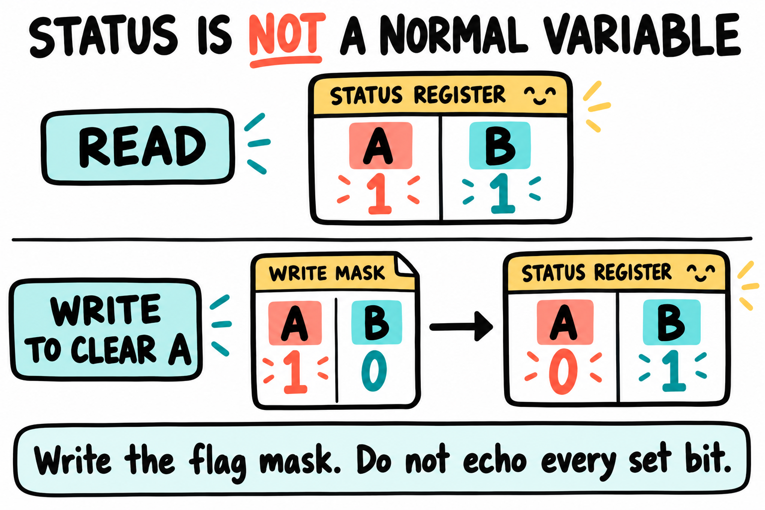
For a W1C register, the write is a request to clear flags, not a replacement status value. Write only the intended clear mask. ECSPI’s TC and RO use this behavior. The I2C flags above are W0C and need a different clear value.¶
A useful checklist is broader than the happy-path register writes:
1. establish ownership and validate board/device requirements
2. prepare power, clock source/gate and pad/input/electrical routes
3. reset or quiesce the controller, with bounded completion checks
4. configure mode, rate, format and clear only the intended status
5. transfer: preserve transaction boundaries and handle errors
6. confirm completion, return buffer ownership, and release resources
An ordinary exclusively owned RW configuration field may permit masked read-modify-write. A FIFO read, a self-clearing command or a W1C/W0C status field has a different contract. Read the field description before choosing the C operator.
Linux separates these responsibilities. An I2C adapter driver operates the controller; an EEPROM client driver requests transactions through it. SPI controller and flash drivers have a similar split. Clock, pinctrl, regulator, locking and DMA APIs coordinate shared resources. You will recognize the hardware sequence, but not every subsystem callback writes a controller register, and not every driver has an identical initialization order.
18.6 Why the bare-metal model ends here¶
Part II gives you a reference model for the boot path: image layout, UART, clocks, DDR, exceptions, timers and translation/cache setup. This optional chapter adds two transaction fragments and a display sketch. Building them is not evidence that a complete production stack has run on your board.
U-Boot now supplies a maintained bootloader structure around these mechanisms. Linux adds process protection, resource ownership and subsystem interfaces. Its early boot does not simply repeat every U-Boot DDR or pin setup. The useful question changes from “which register do I write?” to “which layer owns this request, and what state does it require?”
You could continue building bare-metal networking, USB or filesystems, or adopt an RTOS. Those are substantial separate projects, not a few remaining register examples. For this book’s Linux goal, Part III is the next dependency.
The supplementary choices remain:
18A, Project organization: separate register definitions, board choices, driver interfaces and build dependencies.
18B, Button + beep: distinguish GPIO levels, qualified events and output timing.
18C, Bare-metal RTC: examine SNVS timekeeping and the documented backup-power arrangement.
Read any combination, or proceed to Chapter 19. Keep the small transactions here available as something you can trace when a higher-level request fails.
18.7 Key Notes¶
The controller’s presence does not establish an attached device. EEPROM address width, flash command set and panel timing belong to the actual populated part and routed board, not a generic i.MX6ULL peripheral name.
An I2C random read preserves one transaction across a repeated START. Address
0x50becomes0xA0/0xA1on the wire, and TXAK requests the master’s final NACK rather than reporting a slave ACK.I2C completion, NACK, arbitration loss and failed STOP have distinct recovery implications. Bounded polling limits waiting but cannot force an external device to release a stuck bus.
SPI command and reply share the required chip-select interval. The single 32-bit MSB-first JEDEC burst preserves that boundary, and its low received byte is the last response byte. Controller completion alone does not establish device identity.
W0C and W1C flags require different clear writes. Ordinary configuration read-modify-write is not a general rule for status registers or FIFO accesses.
LCD scan timing, memory packing and device addressing must agree with the panel and memory map. Cache cleaning makes pixels visible, while frame-boundary switching and confirmed completion determine which buffer the CPU may reuse.
Linux controller, client and resource-management layers divide these responsibilities among owners. A bare-metal fragment needs exclusive hardware ownership and is not safe beside a live Linux driver.
The EEPROM and flash transactions above are reads, not update procedures. EEPROM writes require a disposable part or explicitly approved scratch location, preservation of old contents, and write-protect, page-boundary, write-cycle and bounded ACK-polling handling. Do not overwrite byte zero of an unidentified board EEPROM or power-cycle during a write. Do not short or disconnect a powered bus to force a timeout.
18.8 Pitfalls¶
I2C flag semantics: IIF/IAL are W0C here. ECSPI TC/RO are W1C. Using the wrong clear value can leave a stale flag or erase unrelated evidence.
I2C early return: a NACK path still needs to release mastership; arbitration loss is different because hardware has already cleared MSTA. A stuck bus needs recovery policy, not endless retries.
I2C repeated START: obey RM §31.6’s delay before writing I2DR. A barrier orders accesses but does not itself promise two elapsed module-clock cycles.
SPI transaction boundaries: SMC is start control, not chip-select hold. A flash command and reply must share the required select interval.
SPI FIFO/byte order: read RXDATA only when RR is set. For our 32-bit MSB-first burst, response bytes occupy bits 23:16, 15:8 and 7:0; masking with
0xFFgives the last one.LCD visibility versus tearing: maintenance, physical/device addressing, scan timing and buffer ownership all matter. None is replaced by an arbitrary delay.
Missing route or clock: a gate does not choose the source/rate; a mux does not necessarily configure the input daisy or electrical properties. Check the entire path before blaming the peripheral protocol.
Busy waits without an exit: this chapter bounds status polling and treats timer failure as an error. The separate fatal idle loops in the application skeleton are intentional, not peripheral-completion loops.
18.9 Going deeper¶
Supplied IMX6ULLRM Rev. 1: Chapter 31 (I2C), 20 (ECSPI), 34 (eLCDIF), plus 18 (CCM) and 32 (IOMUXC). The book’s chapter numbers are not the RM’s chapter numbers.
Supplied MINI V2.2 schematic, sheet 1 for I2C nets/pull-ups; CORE V2.0 schematic, sheets 6/8 for the UART4/I2C route. Check the actual populated revision before using these routes.
Supplied IMX6ULL errata Rev. 1.2: ERR007805 (I2C low period), ERR009606 (SPI master burst length) and ERR009535 (SPI slave burst termination).
Linux v6.12
i2c-imx.c: controller state, timeouts, recovery and SoC-specific flag semantics.Linux v6.12
spi-imx.c: controller transfers, FIFO handling, clock setup and chip-select policy.Linux v6.12 DRM
mxsfb: display modes and scanout-buffer handling, rather than a universal list of panel writes.
The core bare-metal model is complete.
You now have mechanisms to inspect, and explicit boundaries where board evidence is still required. Carry that habit into U-Boot: trace what the code owns, what it assumes at entry and what its completion check actually proves.
Next, choose: Chapters 18A-18C for supplementary design cases, or Part III, Chapter 19, U-Boot, from source, first boot.