Chapter 9: First LED, pure assembly
The host can already see the board in USB downloader mode. Now we want one observation that comes from our own program: the user LED changing state. No Linux console is involved. The ROM loads a small assembly payload into OCRAM, then gives it control.
An LED seems like a modest reward for all that preparation. It is also a useful first witness. To blink, the program must reach its entry point, access a GPIO controller and route that controller to the right pad. We can inspect each of those steps without first building a C runtime or initializing DDR.
Keep the Chapter 8 power and connector checks in place for any board operation. This example assumes an open development device and a fresh ROM downloader boot, not a jump from U-Boot or another running program. We do not change security fuses. The listings explain that execution path without requiring a board run to continue reading.
9.1 What we are about to build
A program with the following structure:
_start:                          ; ROM jumps here
    set SP to top of OCRAM
    enable clock to GPIO1        ; one write to CCM_CCGR1
    set pin GPIO1_IO03 to ALT5    ; one write to IOMUXC
    configure pad properties     ; one write to IOMUXC
    preload LED-off level        ; set bit 3 in GPIO1_DR
    set GPIO1_IO03 as output     ; one write to GPIO1_GDIR
loop:
    toggle GPIO1_IO03            ; toggle bit 3 of GPIO1_DR
    delay  (busy loop)
    branch loop
There is no scheduler and no hidden GPIO initialization. The listing below contains the instructions and constants we need. Its payload is small, but the padded .imx file will exceed 4 KiB. Do not confuse the code size with the upload file size.
No linker script this chapter. The program is small enough to hand-place. Chapter 10 introduces the linker script as soon as we want C.
On the supplied Point Atom MINI schematic, the user LED is on GPIO1_IO03. It is active-low: its anode receives 3.3 V through a resistor, and the GPIO sinks current to light it. A high output turns it off. Confirm the pad and net on your exact board before uploading. For another pin, look up its mux, pad and GPIO registers again. The clock-gate register may remain the same if the pin belongs to the same bank.
The vendor Linux device tree confirms this mapping. It names the device sys-led and declares GPIO bank 1, bit 3, active-low.
9.2 Clock, pad and output
Think in three jobs rather than three literal writes. This example uses more than three register writes:
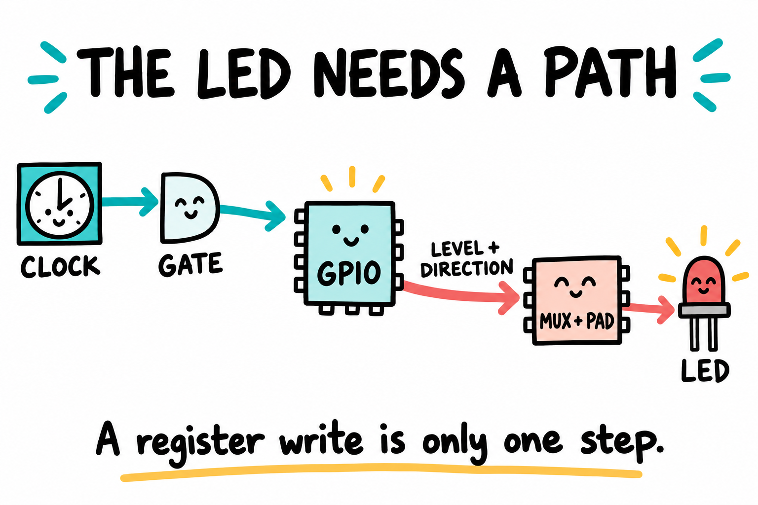
Follow the clock into GPIO, then follow the output toward the LED. Both paths must be ready. The blocks show responsibilities, not separate chips or a count of register writes.
Enable the GPIO controller’s clock, using its two-bit field in
CCM_CCGRx. Do not rely on reads or writes while its required clock is stopped.Route the pin to its GPIO function, by writing the ALT number to
IOMUXC_SW_MUX_CTL_PAD_<padname>. Without this, the pin still belongs to whatever default function the silicon picked at reset (often a different peripheral).Choose the output level and direction. Preload the LED-off level in
GPIO<bank>_DR, then set the bit inGPIO<bank>_GDIRto enable the output. This avoids deliberately exposing an old latch value when the direction changes.
You can also write IOMUXC_SW_PAD_CTL_PAD_<padname> to set drive strength, slew rate, and pulls. We use 0x17059, the pad value from the vendor Linux device tree for this LED pin.
Addresses for GPIO1_IO03, from the Reference Manual:
Register |
Address |
Purpose |
|---|---|---|
|
|
Bits 26:27 (CG13) = GPIO1 clock gate |
|
|
MUX select for pin GPIO1_IO03 |
|
|
Pad properties for pin GPIO1_IO03 |
|
|
GPIO1 data register (bit 3 = our pin, i.e. |
|
|
GPIO1 direction register. Bit 3 = direction for GPIO1_IO03. 1 = output. |
The value to write into MUX_CTL for GPIO function is 5. The IOMUX table in RM Chapter 32 says, for the pad GPIO1_IO03, ALT5 is GPIO1_IO03.
CCM_CCGR encoding (2 bits per gate)
Every CCM_CCGRx register holds 16 clock gates × 2 bits each = 32 bits. The 2-bit field per gate is:
Bits |
Meaning |
|---|---|
|
Clock off in all CPU run modes, peripheral cannot be accessed |
|
Clock on in RUN mode, off in WAIT and STOP, low-power-friendly |
|
Reserved, do not program this value |
|
Clock on in RUN and WAIT, off in STOP |
For this running program, write 0b11 into CG13. Its field occupies bits 26-27, so the mask is 0b11 << 26 = 0x0C000000. OR that mask into the existing value to preserve the other fields. Writing 0xFFFFFFFF would also modify unrelated and reserved fields. Chapter 13 follows the clock upstream. Here we only need its gate.
9.3 The assembly source
In a new host terminal, run . ~/imx6ull/scripts/env.sh, then create ~/imx6ull/src/ch09-asm-led and open it in your editor. Save the following as led.S there. Save the Makefile from Section 9.4 beside it. Lines beginning with $ in command examples show the shell prompt. Do not type the $.
    .syntax unified
    .cpu    cortex-a7
    .arm
    .text
    .global _start

_start:
    cpsid   if, #0x13              @ SVC mode, IRQ and FIQ masked
    /* --------------------------------------------------------------
     *  1. Establish a stack.  The Boot ROM has used part of OCRAM
     *     for its own bookkeeping. This program does not use the stack.
     *     OCRAM ends at 0x00920000 (128 KB starting at 0x00900000).
     *     We set SP just below that.  An LED blink doesn't actually
     *     touch the stack. The ROM has already handed off before this runs.
     * -------------------------------------------------------------- */
    ldr     sp, =0x0091FFF0

    /* --------------------------------------------------------------
     *  2. Enable the GPIO1 clock gate.
     *     CCM_CCGR1 @ 0x020C406C, CG13 = bits 26:27 = 0b11 (RUN/WAIT)
     * -------------------------------------------------------------- */
    ldr     r0, =0x020C406C         @ &CCM_CCGR1
    ldr     r1, [r0]
    orr     r1, r1, #(3 << 26)      @ set CG13 = 0b11
    str     r1, [r0]

    /* --------------------------------------------------------------
     *  3. IOMUX: select ALT5 (GPIO function) for pad GPIO1_IO03.
     * -------------------------------------------------------------- */
    ldr     r0, =0x020E0068         @ &IOMUXC_SW_MUX_CTL_PAD_GPIO1_IO03
    mov     r1, #5
    str     r1, [r0]

    /* --------------------------------------------------------------
     *  4. Configure the pad with the value used by the vendor Linux
     *     device tree for this board's LED pin.
     * -------------------------------------------------------------- */
    ldr     r0, =0x020E02F4         @ &IOMUXC_SW_PAD_CTL_PAD_GPIO1_IO03
    ldr     r1, =0x00017059
    str     r1, [r0]

    /* --------------------------------------------------------------
     *  5. Preload the active-low LED's off level, then enable output.
     * -------------------------------------------------------------- */
    ldr     r0, =0x0209C000         @ &GPIO1_DR
    ldr     r1, [r0]
    orr     r1, r1, #(1 << 3)       @ high = LED off
    str     r1, [r0]

    ldr     r0, =0x0209C004         @ &GPIO1_GDIR
    ldr     r1, [r0]
    orr     r1, r1, #(1 << 3)
    str     r1, [r0]

    /* --------------------------------------------------------------
     *  6. Blink loop. Toggle bit 3 in GPIO1_DR, delay, repeat.
     *     This is only a rough delay. It is intentionally long enough
     *     to remain visible when the CPU clock is faster than expected.
     * -------------------------------------------------------------- */
    ldr     r4, =0x0209C000         @ &GPIO1_DR
    ldr     r5, [r4]                @ current value
    mov     r6, #(1 << 3)           @ bit mask for pin 3

blink:
    eor     r5, r5, r6              @ toggle bit 3 in our saved copy of GPIO1_DR
    str     r5, [r4]                @ write back

    ldr     r7, =50000000         @ long crude delay, not a calibrated interval
1:  subs    r7, r7, #1
    bne     1b

    b       blink

    .end
A few notes on what’s there and what isn’t:
No private exception vectors. We explicitly mask IRQ and FIQ, but those masks do not prevent undefined-instruction or abort exceptions. This first listing assumes valid instructions and accesses. Chapter 10 adds placeholder vectors, and Chapter 15 adds handlers.
No
.data, no.bss. Every value we use is an immediate or computed at run time. Therefore no startup code is needed to copy or zero anything.No
main()._startis the entry. It never returns. An assembly program has no caller to return to. You must explicitly loop forever.ldr r0, =0x...asks GNU assembler to load a constant. It may use an encodable immediate instruction or a PC-relative load from a literal pool. Inspect the disassembly to see which it chose. Arbitrary 32-bit constants do not all fit one ARM immediate instruction.1:is a local label.1bmeans “branch to the nearest1label going backward.” This is a GAS convention for local loops. It avoids us inventing new names..syntax unifiedsays “use the modern ARM/Thumb-unified mnemonics”, which lets us writeorr r1, r1, ...even in ARM mode without surprises.
The delay count is deliberately large. A short loop that looked slow on an MCU may make this LED appear steady. CPU clock, instruction-cache state and branch timing all affect the interval, so do not label it as milliseconds. Reducing the count changes the interval without establishing a calibrated frequency. Chapter 16 supplies a measured timebase.
9.4 Building the image
Two files: led.S and a small Makefile.
# Makefile
CROSS := arm-none-eabi-

all: led.bin

led.o: led.S Makefile
	$(CROSS)gcc -mcpu=cortex-a7 -marm -ffreestanding -c -o $@ $<

led.elf: led.o Makefile
	$(CROSS)ld -Ttext=0x00908000 -e _start -o $@ $<

led.bin: led.elf
	$(CROSS)objcopy -O binary --only-section=.text $< $@

clean:
	rm -f led.o led.elf led.bin led.imx

.PHONY: all clean
What is going on:
-cassemblesled.Sintoled.owithout linking it.-Ttext=0x00908000tells the linker that.textwill run from address0x00908000. The image wrapper below places the first byte ofled.binat exactly that address.-e _startrecords_startas the ELF entry point. The i.MX IVT also uses this same address.--only-section=.textcopies only our code and its literal pool intoled.bin.
From this project directory, build. The commands below the prompt are representative output. The byte count depends on the listing and assembler:
$ make
arm-none-eabi-gcc -mcpu=cortex-a7 -marm -ffreestanding -c -o led.o led.S
arm-none-eabi-ld -Ttext=0x00908000 -e _start -o led.elf led.o
arm-none-eabi-objcopy -O binary --only-section=.text led.elf led.bin
$ wc -c led.bin
Check the ELF before wrapping it:
$ arm-none-eabi-readelf -h led.elf | grep 'Entry point'
  Entry point address:               0x908000

$ arm-none-eabi-objdump -d led.elf | head
00908000 <_start>:
Both commands must show 0x00908000. If they show another address, stop and fix the build before using uuu.
9.5 Wrapping the .bin in an .imx
led.bin is raw machine code. The Boot ROM in SDP mode does not execute raw bins, it executes images that present an IVT (Chapter 7). We need to wrap.
For this chapter, a short Python script places each structure at an exact file offset. Chapter 11 explains and extends this image builder.
Save as wrap.py:
#!/usr/bin/env python3
import struct
from pathlib import Path

IMAGE_START = 0x00907000
IVT_OFFSET  = 0x00000400
CODE_OFFSET = 0x00001000

IVT_ADDR  = IMAGE_START + IVT_OFFSET   # 0x00907400
ENTRY_ADDR = IMAGE_START + CODE_OFFSET # 0x00908000
BOOT_ADDR  = IVT_ADDR + 0x20           # 0x00907420

code = Path('led.bin').read_bytes()
image_size = CODE_OFFSET + len(code)
if not code or IMAGE_START + image_size > 0x00918000:
    raise SystemExit('Payload must be nonempty and fit the ROM-active OCRAM window')

# IVT header: tag, 16-bit big-endian length, version.
ivt = struct.pack('>BHB', 0xD1, 0x0020, 0x40)
ivt += struct.pack('<IIIIIII',
    ENTRY_ADDR, # entry
    0,          # reserved1
    0,          # dcd, none for this OCRAM program
    BOOT_ADDR,  # boot_data
    IVT_ADDR,   # self
    0,          # csf, image is not signed
    0)          # reserved2

# BootData describes the complete image, including the bytes before the IVT.
boot_data = struct.pack('<III', IMAGE_START, image_size, 0)

image = bytearray(b'\x00' * CODE_OFFSET)
image[IVT_OFFSET:IVT_OFFSET + len(ivt)] = ivt
image[IVT_OFFSET + 0x20:IVT_OFFSET + 0x20 + len(boot_data)] = boot_data
image += code

# UUU loads file offset 0x400 at IVT_ADDR. Therefore file offset 0x1000
# lands at IVT_ADDR + (0x1000 - 0x400), which must equal ENTRY_ADDR.
loaded_code_addr = IVT_ADDR + (CODE_OFFSET - IVT_OFFSET)
assert loaded_code_addr == ENTRY_ADDR
assert image[CODE_OFFSET:] == code

Path('led.imx').write_bytes(image)
print(f'IVT:  file 0x{IVT_OFFSET:04X} -> RAM 0x{IVT_ADDR:08X}')
print(f'code: file 0x{CODE_OFFSET:04X} -> RAM 0x{ENTRY_ADDR:08X}')
print(f'size: {len(image)} bytes')
$ python3 wrap.py
IVT:  file 0x0400 -> RAM 0x00907400
code: file 0x1000 -> RAM 0x00908000
size: ... bytes
Your size may differ slightly. The two addresses must match the output above.
The important layout is:
File offset |
Loaded RAM address |
Content |
|---|---|---|
|
Not uploaded by UUU |
Padding used by SD and eMMC boot images |
|
|
IVT |
|
|
BootData |
|
|
Padding |
|
|
First instruction in |
If you decode the IVT now you should see exactly the values we set:
$ xxd -s 0x400 -l 32 led.imx
00000400: d100 2040 0080 9000 0000 0000 0000 0000  .. @............
00000410: 2074 9000 0074 9000 0000 0000 0000 0000   t...t..........
Tag D1 00 20 40, entry 00 80 90 00 (little-endian → 0x00908000), dcd zero, boot_data 20 74 90 00 (→ 0x00907420), self 00 74 90 00 (→ 0x00907400). Matches.
9.6 Pushing to the board with uuu
Follow Chapter 8’s checked power-down and power-up procedure. Set the boot-mode switch to SDP (USB-Downloader) while the board is unpowered. Account for all attached power sources and UART back-power paths.
Connect the USB-OTG cable to the host.
Power on.
Confirm enumeration:
$ lsusb | grep 15a2
Bus 001 Device 010: ID 15a2:0080 Freescale SemiConductor Inc i.MX 6 SystemOnChip in RecoveryMode
Push the image:
$ sudo "$IMX6ULL_HOME/build/mfgtools/uuu/uuu" led.imx
... release/banner output varies; the following is the expected command shape ...

Success 1    Failure 0
3:2-         2/ 2 [Done                                  ] SDP: done
When the argument is an image instead of a UUU command file, uuu automatically creates this command:
SDP: boot -f <image>
UUU then performs these steps:
Find the IVT at file offset
0x400.Upload from that offset to
IVT.self, which is0x00907400.Ask the ROM to process the IVT at
0x00907400.The ROM reads
IVT.entryand branches to_startat0x00908000.
Success 1 Failure 0 means that the USB transfer and ROM commands succeeded. It does not prove that _start contains valid code at the entry address.
Watch the LED. It should blink.
If it does not:
Check all three execution addresses.
readelf,objdump, andwrap.pymust all show_startat0x00908000.Check the image layout.
wrap.pymust report code at file offset0x1000and RAM address0x00908000.Check the LED’s pin. This code controls
GPIO1_IO03. Confirm that this is the user LED in your exact board revision.Check the blink delay. A very short delay makes the LED look continuously on or dim. The constant is not a promised half-second interval.
Power-cycle and retry. After the ROM jumps to your program, it cannot accept another SDP upload until the board resets.
9.7 What happened, step by step
If you got the blink, this sequence ran on real silicon:
Power on
  → Boot ROM runs from internal ROM at 0x00000000
    → reads BOOT_MODE pins, sees SDP
    → enumerates as USB device 15a2:0080
    → waits for host commands
host: uuu pushes led.imx over USB
  → UUU skips the file's first 0x400 bytes
  → ROM receives the IVT and following bytes at RAM 0x00907400
  → ROM receives JUMP_ADDRESS: 0x00907400
ROM:
  → finds IVT signature 0xD1 at 0x00907400
  → reads IVT.dcd (zero, skip DCD)
  → reads IVT.entry = 0x00908000, jumps there
Your code:
  → _start sets SP
  → enables GPIO1 clock gate
  → sets pin ALT5
  → sets pin direction = output
  → enters blink loop
LED blinks. The ROM executed first. From the handoff into `_start`, the instructions controlling this LED are ours.
No software layer sits between this program and the chip. The next chapters add layers on top of this direct register-access model.
9.8 Key Notes
The ROM owns loading and the initial handoff. The assembly payload owns the GPIO configuration after entry, with no C runtime, scheduler or DDR dependency.
The clock gate, mux selection and output latch/direction serve different purposes. A writable GPIO register does not establish that its signal reaches the intended pad.
Preloading the active-low LED’s off level before enabling output avoids exposing a stale latch value. Active-low polarity does not imply an open-drain driver.
The ELF entry, IVT entry and loaded code location must agree. USB command success establishes a transfer result, not execution of the intended instructions.
A busy-loop delay depends on clock and instruction timing. Its count is not a duration, and rapid toggling can look like a steady LED.
A header pin is not automatically a spare output. Its voltage domain, connected loads and boot role constrain use. Never drive a supply, connected output or boot strap as though it were an LED connection.
9.9 Pitfalls
Forgetting the CCGR write. Confirm the required gate before interpreting register accesses. A stopped-clock access does not have one universal, safe failure value.
Wrong IOMUX ALT. Symptom: writes to GPIO_DR succeed but the pin doesn’t move. Some pads default to “GPIO” in their reset ALT. Many do not. Always set ALT explicitly.
Entry address does not match code location. Symptom:
uuureports success, but the board does nothing. The host cannot tell whether valid instructions exist atIVT.entry. Check the file-to-RAM map in Section 9.5.Delay is too short. The LED may look continuously on even though the pin is toggling quickly.
Resetting after a successful upload. This image is in RAM. A new downloader boot waits for another upload. The SDP path leaves persistent storage unchanged. Switching to SD requires a separately prepared and verified bootable card as described in Chapter 11.
Mistaking active-low for open-drain. Active-low describes which level lights the LED. Open-drain describes the output driver. They are different properties. Our pad setting uses a push-pull output.
Optimization eating your loop. GCC with
-O2may unroll or completely eliminate a delay loop with no side-effects. We avoided this here by leaving the loop in raw asm. If you port to C, mark the countervolatile.
9.10 Going deeper
IMX6ULLRM Chapter 28, GPIO: Specifically Table 28-1 (register summary) and Table 28-3 (GPIOx_DR bit layout).
IMX6ULLRM Chapter 32, IOMUXC: Look up GPIO1_IO03 in the IOMUX table.
IMX6ULLRM Chapter 18, CCM: Table 18-3 (gate encoding) and Section 18.6.24 (
CCM_CCGR1). Table 18-5 in Chapter 8 is the ROM’s disabled-clock list, not the gate-encoding table.ARM DDI 0406 Section A8.8.62,
LDR (literal)form, which is whatldr Rn, =constexpands into.The GNU Assembler manual, “ARM Dependent Features”,
.syntax unified,.cpu,.global, literal pools.Your Point Atom MINI schematic, the only authoritative source for which LED is on which pin on your board.
The LED is a simple execution witness in this design. Chapter 10 keeps the same output path and changes the language, supplying the stack and memory initialization that C expects before main() can run.