Chapter 13: CCM clock tree bring-up
A UART can print perfectly while your clock calculation is wrong. Its baud rate depends on the UART root, not directly on the ARM core. Before changing speed, answer a smaller question: which path supplies each clock right now?
This chapter builds a read-only clock audit, then explains what a clock transition requires. Actual frequency/voltage changes remain part of the board-qualified startup sequence. Begin with the handoff state: a ROM, DCD, or loader may have changed the reset configuration.
Operating-point prerequisite: identify the fitted CPU speed grade, supply voltage, temperature range, and board revision using Chapter 5. PLL lock does not authorize 696 or 792 MHz. The
05marking in the supplied core schematic is a 528 MHz-grade part. Do not raise frequency to discover whether a part survives it.
13.1 What we want to set up
This example plan names the parent and divider behind each domain. It is a worked clock tree, not an instruction to apply these frequencies.
Domain |
Example frequency |
Conditions needed |
|---|---|---|
ARM core |
396 MHz |
PLL1 = 792 MHz, ARM divider = 2; allowed operating point |
AHB |
132 MHz |
|
IPG |
66 MHz |
AHB / 2 |
AXI |
198 MHz |
AXI selects |
UART |
80 MHz |
PLL3 = 480 MHz, fixed /6 path, UART divider = 1 |
MMDC |
396 MHz |
|
Notice the extra 2 in periph2_clk. On i.MX6ULL, MMDC is not simply
the AHB parent divided again. Sharing PLL2_PFD2 still creates a dependency:
changing that PFD can disturb both buses and working DDR.
For a hypothetical, permitted 696 MHz ARM operating point, PLL1 divider 58
and ARM divider 1 give 24 MHz * 58 / 2 = 696 MHz. That arithmetic says
nothing about the regulator setting or safe transition sequence.
13.2 The ANATOP block, PLLs and PFDs
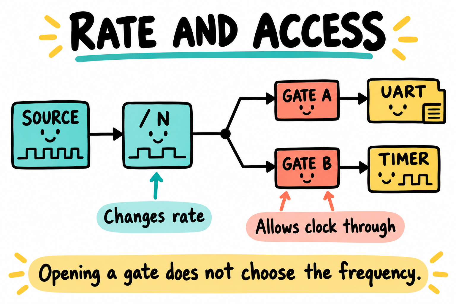
A gate controls whether a clock passes. It does not select its rate. The shared branch is a conceptual example, not the actual UART and timer root topology. Follow each real root in the register map below.
Analog clock registers occupy the region at 0x020C8000. The supplied
reference manual describes them in Chapter 18, alongside CCM.
Register |
Offset |
Role |
|---|---|---|
|
|
PLL1 |
|
|
PLL3 |
|
|
PLL7 |
|
|
PLL2 |
|
|
PLL5 |
|
|
PLL6 |
|
|
PLL3 PFDs |
|
|
PLL2 PFDs |
Registers that document SET/CLR/TOG aliases have them at +4/+8/+12. Observe each register’s reserved-bit rules. An atomic write cannot make an unsafe clock transition safe.
PLL1 (ARM PLL)
Bits |
Field |
Meaning |
|---|---|---|
6:0 |
DIV_SELECT |
Range 54..108; |
12 |
POWERDOWN |
1 powers down the PLL |
13 |
ENABLE |
Enables output |
15:14 |
BYPASS_CLK_SRC |
0 selects the 24 MHz reference |
16 |
BYPASS |
Selects bypass instead of PLL output |
31 |
LOCK |
Lock status, not operating-point approval |
The ARM root also selects PLL1 or step_clk in CCSR. Reading only the PLL
divider and CACRR misses that mux and PLL bypass.
PLL2 (System PLL)
Normal operation uses 528 MHz. The register also offers 480 MHz:
DIV_SELECT=0 selects 20 * f_ref; 1 selects 22 * f_ref
(528 MHz). Reversing those encodings gives plausible but wrong answers.
A PFD generates f_PLL * 18 / FRAC, with FRAC in the documented 12..35 range.
For a 528 MHz parent:
PFD |
Example FRAC |
Calculated frequency |
|---|---|---|
PFD0 |
27 |
352 MHz |
PFD1 |
16 |
594 MHz |
PFD2 |
24 |
396 MHz |
PFD3 |
32 |
297 MHz |
Each eight-bit PFD lane contains FRAC, a stable indication, and a gate. Before writing FRAC, follow the documented gating sequence and detach or quiesce consumers. An OCRAM function must not casually edit a live DDR source.
PLL3 (USB1 PLL, also feeds peripherals)
Normal operation uses 480 MHz. Its POWER bit has the opposite sense from PLL1/PLL2 POWERDOWN: bit 12 must be 1 for power. PLL3 has PFDs, but the UART mux selects PLL3 / 6 or the oscillator, not a PFD. The UART post-divider then divides the selected source.
13.3 The CCM block, root clocks and gates
CCM base is 0x020C4000.
Register |
Offset |
Purpose |
|---|---|---|
|
|
Oscillator control |
|
|
ARM step/PLL selection |
|
|
ARM post-divider |
|
|
Bus dividers and final muxes |
|
|
Bus parent muxes |
|
|
PERCLK and other roots, not UART selection |
|
|
UART source/divider, USDHC dividers |
|
|
Clock transition busy flags |
|
|
Peripheral gates |
Divider fields usually encode divisor - 1. Handshakes have separate bits:
CDHIPR bit |
Transition |
|---|---|
0 |
AXI divider |
1 |
AHB divider |
2 |
MMDC divider |
3 |
|
5 |
|
16 |
ARM divider |
A transition routine must wait for its own busy bit, with a failure path. Polling bits 0..2 does not wait for ARM. Some mux changes require consumers to be inactive and gated; a handshake poll does not waive those requirements (RM sections 18.6.6, 18.6.7, 18.6.17).
13.4 The bring-up code
These files are a compilable audit module, not a clock initializer.
Use Chapter 10’s integer-only flags:
-mcpu=cortex-a7 -marm -mfloat-abi=soft -mgeneral-regs-only -ffreestanding.
Use matching architecture flags when linking and link -lgcc after objects
for the wide division helper. Add clocks.o to the existing build.
Preconditions: MMU-off physical access, a 24 MHz reference, privileged execution, and a stable clock tree. Keep IRQs masked during the audit. Zero means unsupported or unavailable, not necessarily a stopped clock. This deliberately rejects external PLL references, the secondary ARM step path, and MMDC’s audio-PLL path instead of guessing their rates.
clocks.h:
#ifndef CLOCKS_H
#define CLOCKS_H
#include <stdint.h>
uint32_t clocks_get_arm_hz(void);
uint32_t clocks_get_ahb_hz(void);
uint32_t clocks_get_ipg_hz(void);
uint32_t clocks_get_uart_hz(void);
uint32_t clocks_get_mmdc_hz(void);
#endif
clocks.c:
#include "clocks.h"
#define REG(a) (*(volatile uint32_t *)(uintptr_t)(a))
#define CCM_CCSR    0x020C400Cu
#define CCM_CACRR   0x020C4010u
#define CCM_CBCDR   0x020C4014u
#define CCM_CBCMR   0x020C4018u
#define CCM_CSCDR1  0x020C4024u
#define CCM_CDHIPR  0x020C4048u
#define PLL_ARM    0x020C8000u
#define PLL_USB1   0x020C8010u
#define PLL_SYS    0x020C8030u
#define PFD_528    0x020C8100u
#define XTAL_HZ    24000000u

static uint32_t pll_hz(uint32_t address)
{
    uint32_t v = REG(address);
    if (address == PLL_USB1 && ((REG(CCM_CCSR) & 1u) || (v & 3u) > 1u))
        return 0; /* unsupported PLL3 test switch/reserved divider */
    if ((v >> 14) & 3u) return 0; /* unsupported reference */
    if (v & (1u << 16)) return XTAL_HZ;
    if (!(v & (1u << 13)) || !(v & (1u << 31))) return 0;
    if (address == PLL_USB1) {
        if (!(v & (1u << 12))) return 0;
    } else if (v & (1u << 12)) {
        return 0;
    }
    if (address == PLL_ARM) {
        uint32_t div = v & 0x7Fu;
        if (div < 54 || div > 108) return 0;
        return XTAL_HZ * div / 2u;
    }
    return XTAL_HZ * ((v & 1u) ? 22u : 20u);
}

static uint32_t pfd_hz(unsigned lane)
{
    uint32_t v = (REG(PFD_528) >> (8u * lane)) & 0xFFu;
    uint32_t frac = v & 0x3Fu;
    uint32_t parent = pll_hz(PLL_SYS);
    if ((v & 0x80u) || !(v & 0x40u) || frac < 12 || frac > 35)
        return 0;
    return (uint32_t)((uint64_t)parent * 18u / frac);
}

static uint32_t periph_hz(void)
{
    uint32_t d = REG(CCM_CBCDR), m = REG(CCM_CBCMR);
    if (d & (1u << 25)) {
        uint32_t sel = (m >> 12) & 3u;
        uint32_t parent = sel == 0 ? pll_hz(PLL_USB1) :
                          sel == 1 ? XTAL_HZ :
                          sel == 2 && !(REG(PLL_SYS) & (3u << 14)) ? XTAL_HZ : 0;
        return parent / (((d >> 27) & 7u) + 1u);
    }
    switch ((m >> 18) & 3u) {
    case 0: return pll_hz(PLL_SYS);
    case 1: return pfd_hz(2);
    case 2: return pfd_hz(0);
    default: return pfd_hz(2) / 2u;
    }
}

uint32_t clocks_get_arm_hz(void)
{
    if (REG(CCM_CDHIPR)) return 0;
    uint32_t s = REG(CCM_CCSR);
    uint32_t parent = (s & (1u << 2)) ?
                     ((s & (1u << 8)) ? 0 : XTAL_HZ) : pll_hz(PLL_ARM);
    return parent / ((REG(CCM_CACRR) & 7u) + 1u);
}

uint32_t clocks_get_ahb_hz(void)
{
    if (REG(CCM_CDHIPR)) return 0;
    return periph_hz() / (((REG(CCM_CBCDR) >> 10) & 7u) + 1u);
}

uint32_t clocks_get_ipg_hz(void)
{
    return clocks_get_ahb_hz() / (((REG(CCM_CBCDR) >> 8) & 3u) + 1u);
}

uint32_t clocks_get_uart_hz(void)
{
    if (REG(CCM_CDHIPR)) return 0;
    uint32_t v = REG(CCM_CSCDR1);
    uint32_t parent = (v & (1u << 6)) ? XTAL_HZ : pll_hz(PLL_USB1) / 6u;
    return parent / ((v & 0x3Fu) + 1u);
}

uint32_t clocks_get_mmdc_hz(void)
{
    if (REG(CCM_CDHIPR)) return 0;
    uint32_t d = REG(CCM_CBCDR), m = REG(CCM_CBCMR), parent;
    if (d & (1u << 26)) {
        parent = (m & (1u << 20)) ? XTAL_HZ : pll_hz(PLL_USB1);
        parent /= (d & 7u) + 1u;
    } else {
        switch ((m >> 21) & 3u) {
        case 0: parent = pll_hz(PLL_SYS); break;
        case 1: parent = pfd_hz(2); break;
        case 2: parent = pfd_hz(0); break;
        default: return 0; /* audio PLL path not decoded here */
        }
    }
    return parent / (((d >> 3) & 7u) + 1u);
}
Each peripheral initializer owns its CCGR gates. For later integration,
keep the two APIs separate: these getters inspect clocks; a board-owned
startup sequence changes them. This module has no clocks_init() entry.
13.5 Verifying with printf
This main-body fragment reports the audit through the Chapter 12 UART interface. Its use assumes that console’s clock and initialization contract:
printf("ARM=%u AHB=%u IPG=%u UART=%u MMDC=%u Hz\r\n",
       clocks_get_arm_hz(), clocks_get_ahb_hz(), clocks_get_ipg_hz(),
       clocks_get_uart_hz(), clocks_get_mmdc_hz());
For section 13.1’s example tree, the calculated values would be 396000000, 132000000, 66000000, 80000000, and 396000000. These are representative calculations, not captured board output or a promised ROM state.
For the IPG calculation, SYS DIV_SELECT=1, PFD2 FRAC=24,
PRE_PERIPH_CLK_SEL=1, PERIPH_CLK_SEL=0, AHB_PODF=2, IPG_PODF=1 give:
24 * 22 * 18 / 24 / 3 / 2 = 66 MHz. The final mux matters too.
13.6 Verifying with hardware
The decoder calculates frequency from fields. It does not measure the oscillator or establish electrical margin.
Quick check: blink rate
A busy-loop blink is a coarse comparison. Optimization, caches, memory stalls, and peripheral bus speed affect it. Going from 396 to 696 MHz is about 1.76, not 2; a GPIO loop need not scale by that ratio.
Better check: count cycles with PMU
This privileged C fragment enables and resets CCNT and clears its
divide-by-64 setting. It does not grant user-mode access. Include stdint.h.
static inline void pmu_cycles_init(void)
{
    uint32_t v;
    __asm__ volatile ("mrc p15, 0, %0, c9, c12, 0" : "=r"(v));
    v = (v & ~(1u << 3)) | 1u | (1u << 2); /* D=0, E=1, C=1 */
    __asm__ volatile ("mcr p15, 0, %0, c9, c12, 0" :: "r"(v) : "memory");
    v = 1u << 31;
    __asm__ volatile ("mcr p15, 0, %0, c9, c12, 1\n\tisb"
                      :: "r"(v) : "memory");
}

static inline uint32_t pmu_ccnt(void)
{
    uint32_t v;
    __asm__ volatile ("isb\n\tmrc p15, 0, %0, c9, c13, 0"
                      : "=r"(v) :: "memory");
    return v;
}
CCNT tells you cycles, not Hz. The same cycle count at two operating
points says nothing about seconds without a time reference. At 696 MHz a
32-bit counter wraps in about 6.17 seconds. Account for interrupts, read
overhead, and security/debug controls. For memory-completion timing, place
an appropriate dsb before the endpoint; isb alone does not drain stores.
Hardware check: scope a GPIO
Use a known, safely routed output and a low-rate waveform. Do not infer CPU cycles from C statement count or try a 70 MHz LED-pin waveform. GPIO read-modify-write travels through the peripheral bus and may be the bottleneck. A timer output or approved CCM clock-output route is more useful if mux, divider, loading, and measurement limits are recorded.
13.7 Why we set up clocks before DDR
Software converts nanoseconds and minimum DDR CK cycle requirements into MMDC register encodings. Choosing the clock comes first; the encoded timings describe that choice.
At 396 MHz, tCK = 2.525... ns. A hypothetical 15 ns minimum requires
ceil(15 / tCK) = 6 cycles, before applying that field’s encoding and
minimum-cycle rules. AHB/IPG govern bus/register access, not this conversion.
Establish the MMDC parent/divider before enabling DRAM. A live DDR clock change requires the documented quiesce/self-refresh transition and errata handling, with code, data, stacks, and other masters kept away from DDR as required. It is not an extra write in this audit module.
13.8 Key Notes
A frequency belongs to a complete selected path: reference, PLL or bypass, PFD where used, muxes and dividers. CCGR gates control availability, not rate.
The audit getters inspect a stable tree. Board startup owns transitions, voltage sequencing and consumer coordination. A zero from this decoder can mean an unsupported path rather than a stopped clock.
Shared parents create shared risks. Changing PLL2_PFD2 can affect buses and MMDC even when the ARM core has moved to another source.
SYS DIV_SELECT=0 with a 24 MHz reference gives 480 MHz. With PFD2 FRAC=24, that becomes 360 MHz rather than the 396 MHz of the 528 MHz parent case.
PLL lock is not operating-point approval. Safe transitions also depend on speed grade, rail voltage, temperature, consumer state and the correct handshake’s bounded failure path.
MMDC timings describe a chosen DDR CK. Changing a live DDR clock requires the documented quiesce/self-refresh protocol, not an isolated divider write.
Register decoding calculates nominal frequency and PMU CCNT counts cycles. Neither establishes elapsed time or electrical margin without an appropriate independent reference or measurement.
13.9 Pitfalls
Lock as permission. Lock does not establish speed grade, voltage, thermal limits, or stable DDR.
Reading only a divider. Mux and bypass may select another parent.
Changing a shared PFD. MMDC can fail even while ARM uses the oscillator.
Wrong handshake. ARM uses CDHIPR bit 16; buses and muxes differ.
Wrong PFD formula. It is
f_PLL * 18 / FRAC; use a wide intermediate.Undoing a DCD. DDR may already be initialized. Audit it before choosing which component owns further changes.
13.10 Going deeper
IMX6ULLRM Chapter 18, sections 18.6.4..7, 18.6.17 and 18.7: muxes, handshakes, PLL/PFD fields.
The fitted part’s i.MX6ULL data sheet: frequency/voltage/temperature conditions. PLL divider range is not a speed-grade table.
U-Boot v2025.01 clock.c: compare
get_periph_clk,get_mmdc_ch0_clk, andget_uart_clk; note the i.MX6UL/ULL-specific branches.Linux v6.12 clk-imx6ul.c: the hardware expressed as clock parents and operations.
Cortex-A7 TRM, performance-monitor chapter: counter controls and access restrictions; this CPU PMU is not the SoC regulator block.
Next chapter: Chapter 14: DDR3 initialization with MMDC. Use the actual clock and fitted geometry to understand a board-specific initialization, without treating copied constants as a working BSP.