Chapter 5: A tour of the i.MX6ULL SoC
A correct register write need not produce a change at a connector. A UART can be configured while its signal is routed to a different pad. A GPIO value can change while the LED’s pad is assigned to another function. The instruction did its job; the path to the outside world was incomplete.
On a new MCU, you would trace that path through the reference manual and schematic. We will do the same on the i.MX6ULL: find the controller, find its clock, and follow its signal to the board. The chip is larger, but the questions are familiar. Keep an LED and a UART in mind as we move through the map; the worked UART1 lookup at the end will bring the pieces together.
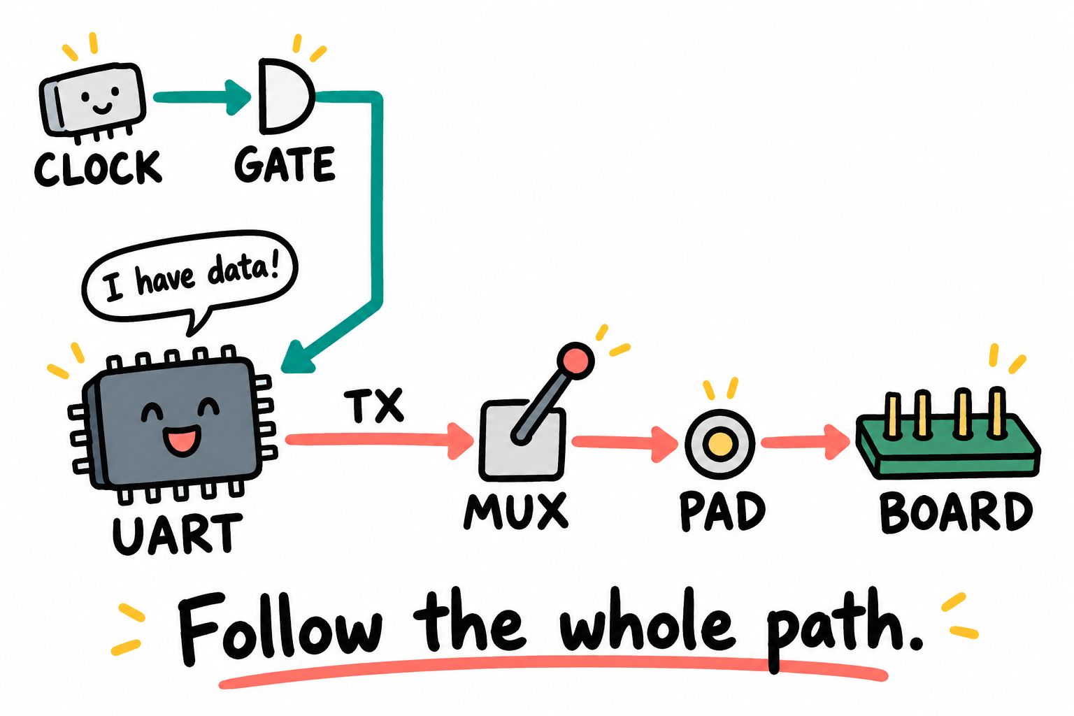
“I have data!” is only the UART’s part. Teal follows the clock into the UART. Coral follows TX out through the selected mux and pad to the board net. The chapter follows both paths. This sketch shows the idea, not the board’s complete wiring.
5.1 What is the i.MX6ULL
The i.MX6ULL is a system on chip, or SoC: the CPU core is one part of a device that also includes memory controllers, clocks, and peripherals. It is a low-cost member of NXP’s i.MX6 family, with one Cortex-A7 and no GPU, VPU, or PCIe controller.
Many of its peripheral names will be familiar: UART, I2C, SPI, timers, and GPIO. Others serve the larger system: the external DDR controller, Ethernet, USB, and storage interfaces. The chip also provides LCD, CSI camera, and SAI audio interfaces. These resources suit systems such as industrial control panels, meters, and gateways.
Keep the following summary nearby as we examine the map. Where a resource depends on the part variant or fitted components, check the actual board rather than relying on the MINI name alone:
Core: one Cortex-A7; permitted frequency depends on the fitted part’s speed grade and supplies.
L1 cache: 32 KB I + 32 KB D
L2 cache: 128 KB unified, integrated inside the Cortex-A7 MPCore (no external PL310 controller)
On-chip memory: 128 KB OCRAM at
0x00900000, plus a separate 96 KB Boot ROM at0x00000000that is mask-programmed by NXP. There is no TCM. A-profile systems normally use caches and system RAM instead.DRAM: 16-bit LPDDR2/DDR3L/DDR3 controller (MMDC). The Point Atom core boards used in this book have 256 MiB or 512 MiB.
Boot media: SD/MMC, eMMC, NAND, SPI NOR, QSPI, parallel NOR, and USB SDP recovery
Process: 28 nm
Package: 289-ball VM (14 x 14 mm) or 272-ball VK (9 x 9 mm), according to the fitted variant/datasheet; not a universal interchangeable pinout.
Before we choose a clock setting, the chip marking deserves a closer look. Two boards sold under a similar name need not carry the same part. Y identifies i.MX6ULL, while G identifies i.MX6UL; those are different families, not price grades of the same part. Within ULL, Y0, Y1, and Y2 identify baseline, reduced-feature, and full-feature variants.
For example, the supplied core schematic labels U1 MCIMX6Y2CVM05AB:
Field |
Meaning in the supplied industrial datasheet |
|---|---|
|
Production qualification |
|
i.MX6ULL family |
|
Full-feature differentiator |
|
Industrial junction-temperature grade |
|
14 x 14 mm MAPBGA package |
|
528 MHz speed grade |
|
Fuse-option field |
|
Silicon revision 1.1 |
The 05 in that long name changes a practical decision: this example is a 528 MHz-grade part. A clock value copied from another project is not made safe by the fact that both projects use a Cortex-A7. Check the marking actually fitted on your board, not just the schematic label. Do not apply a 696 MHz example to a 528 MHz-grade part. Even a higher-grade part needs the documented voltage and temperature conditions for its chosen frequency.
5.2 Block diagram
Here is a simplified view of how the major blocks connect. Some buses are omitted so we can follow the path from the CPU to memory and peripherals:
                  ┌─────────────────────────────────────────────┐
                  │             Cortex-A7 (1 core)              │
                  │   L1-I 32KB │ L1-D 32KB │ NEON │ VFPv4      │
                  └────────────┬────────────────────────────────┘
                               │ AXI
   ┌───────────────────────────┼────────────────────────────────┐
   │                         BUS MATRIX (AXI/AHB/IPS)           │
   └─┬───────┬────────────┬──────────────┬────────┬─────────────┘
     │       │            │              │        │
     ▼       ▼            ▼              ▼        ▼
   OCRAM   ROM         MMDC            EIM      Peripherals
   128KB   96KB        DDR ctrl    parallel mem  via IPS bus
                       │
                       ▼
                   external DDR3
                   (256/512 MB on MINI)
Follow a line from the CPU to OCRAM, then follow another toward the peripherals. The bus matrix carries those accesses from a master, such as the CPU or a DMA engine, to the selected target. A UART register write travels out of the core to the controller’s block. The early examples do not configure the matrix, but it makes the next table more concrete: the physical address selects where that access goes.
5.3 System memory map
Where does a CPU load or store go? The physical address selects a region in the SoC’s 4 GiB map. Some regions contain memory, others contain registers, and others are reserved. This selected-region table follows RM Tables 2-1 through 2-4; an address marked reserved is not spare space for our code.
Region |
Base |
Size |
What’s there |
|---|---|---|---|
Boot ROM |
|
96 KB |
NXP’s mask-programmed boot code (see Ch 7) |
OCRAM |
|
128 KB |
On-chip SRAM |
GIC distributor |
|
4 KB |
(and CPU interface at |
External PL310 L2 controller |
(absent) |
- |
i.MX6ULL’s 128 KB L2 is integrated in the MPCore block. |
AIPS-1 |
|
1 MB region |
Includes GPIO, UART1, IOMUXC, CCM/analog clocks, GPT/EPIT, SNVS |
AIPS-2 |
|
1 MB region |
Includes USB, MMDC, USDHC and other peripheral blocks |
AIPS-3 |
|
1 MB region |
Includes DCP, RNGB, UART8, EPDC and related blocks |
External Memory Interface (EIM) |
|
128 MB |
Parallel external memory; alias at |
QSPI |
|
256 MB |
Memory-mapped QuadSPI flash |
MMDC0 (DRAM) |
|
up to 2 GB |
External DDR3 |
For the early boot designs, three parts of the map are especially useful. First, DRAM begins at 0x80000000. A U-Boot setting such as loadaddr=0x80800000 therefore places an image 8 MiB above that base, leaving working space around it. Remember that this is external memory and needs initialization before use.
This creates a boot problem worth noticing. A board may have hundreds of megabytes of DDR, yet our first program cannot assume it is usable. Something must configure its controller first. OCRAM begins at 0x00900000 and gives us on-chip SRAM before DDR is ready. Our first bare-metal images run there. A small U-Boot SPL, or Secondary Program Loader, can also begin there, initialize DDR, and load a larger stage.
Third, most peripheral registers lie in AIPS-1, AIPS-2, or AIPS-3. For example, the Clock Controller Module, CCM, starts at 0x020C4000, inside AIPS-1. The high address digits help you identify the containing region, but use the block’s own register table for the exact address.
The full map is RM Chapter 2. In particular, 0x00018000-0x000FFFFF, 0x00100000-0x00107FFF, and the region containing 0x08000000 are reserved, not the ROM aliases or EIM base sometimes listed for other configurations.
5.4 OCRAM and the boot footprint
OCRAM solves the first-memory problem, but there is a catch in its budget. The chip provides 128 KB; the Boot ROM leaves only about 68 KB free while it is loading. Both numbers are correct. The ROM is a running program with its own memory needs. RM 8.4.1, Figure 8-3 gives the boundaries below; it does not assign further subdivisions within the lower reservation.
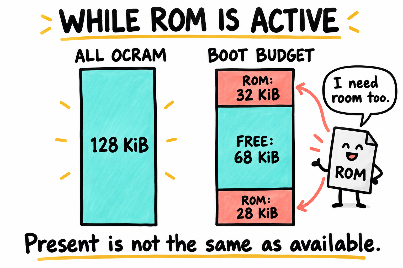
The coral regions are RAM reserved for the ROM’s work, not the ROM storage itself. While the ROM is running, our image must fit between them. The table below gives the exact addresses. The drawing is not to scale, and these reservations are not a permanent post-handoff limit.
Start |
End |
Approx size |
During Boot ROM execution |
What it means for us |
|---|---|---|---|---|
|
|
28 KiB |
Reserved. |
Do not load over it while ROM is active. |
|
|
68 KiB |
OCRAM free area. |
Image headers, loaded payload, and any concurrent allocations must fit. |
|
|
~32 KB |
ROM MMU table, stack, and per-boot state. |
Reserved until the ROM has handed off. |
During Boot ROM execution, the usable window is the ~68 KB middle range. After the ROM transfers control and its services are no longer needed, software can use the entire 128 KB OCRAM range, 0x00900000-0x0091FFFF.
That gives our loader a different limit from the physical memory limit: loaded bytes must remain below 0x00918000, not merely below 0x00920000. In the first padded image, we use 0x00907000 as the image base, 0x00907400 for the IVT header, and 0x00908000 for the code entry. Chapters 6 and 7 show how those choices fit together.
The time at which we use the memory matters as much as its address. We cannot borrow the ROM’s stack while the ROM is still using it to load our image. Budget the loaded bytes and our own stack explicitly; the linker script in Chapter 6 will turn that boundary into a build check.
5.5 The clock tree (at one level of detail)
Return to the UART whose correct register writes did not produce output. Finding its address tells us where to write, but the block also needs a clock. The full clock tree has roughly 200 leaf signals. We can make a useful start without following all of them: trace one source through the tree to the peripheral we need.
External oscillators ─► PLLs (ANATOP) ─► Root clocks (CCM) ─► Gates (CCGR) ─► Peripherals
Layer 1, Oscillators
XTALOSC24M: the 24 MHz crystal reference for the main clock tree. The Point Atom MINI has a 24 MHz crystal on Y2.
XTALOSC32K: 32.768 kHz crystal for the RTC / SNVS domain. Optional. If absent, the RTC is less accurate.
Layer 2, PLLs (in the ANATOP block)
Seven PLLs:
PLL |
Example output/rate |
Purpose |
|---|---|---|
PLL1, ARM PLL |
Depends on DIV_SELECT |
Feeds ARM root through downstream division; not automatically the final core rate |
PLL2, System PLL |
528 MHz normal intended rate |
Bus clocks, peripherals; a selection field is not approval for arbitrary rates |
PLL3, USB1 PLL |
480 MHz normal intended rate |
USB, peripheral references |
PLL4, Audio PLL |
variable (44.1/48 kHz multiples) |
SAI |
PLL5, Video PLL |
variable (LCD pixel rates) |
eLCDIF |
PLL6, ENET PLL |
500 MHz internal PLL rate |
Divided reference outputs serve Ethernet; this is not a 500 MHz PHY reference |
PLL7, USB2 PLL |
480 MHz |
Host USB |
A PLL, or Phase-Locked Loop, produces faster clocks from a reference. PLL2 and PLL3 also expose four PFDs, Phase Fractional Dividers, per PLL. These provide divided outputs; PLL2_PFD2 at 396 MHz, for example, is commonly used as a source in the AHB clock path.
Layer 3, Root clocks (in CCM)
The CCM selects among PLL and PFD outputs and applies dividers to produce named root clocks. Names such as AHB_CLK_ROOT, IPG_CLK_ROOT, and UART_CLK_ROOT tell you which part of the system they serve. There are roughly 60 of these roots; we follow the one needed by a peripheral rather than configuring them all at once.
The following rates illustrate a later configuration, subject to the fitted part’s limits. They are not the frequencies to assume just after reset:
ARM core: 696 MHz (PLL1)
AXI bus: 198 MHz (PLL2_PFD2 / 2)
AHB: 132 MHz
IPG (peripheral bus): 66 MHz
UART input: 80 MHz (PLL3 / 6)
Chapter 13 performs the explicit clock setup. Before then, our ROM-loaded program inherits the ROM’s starting state described in RM 8.4.3, not a configuration from U-Boot. When checking a frequency, follow its source and divider: a PLL’s output rate is not necessarily the rate reaching the CPU or peripheral.
Layer 4, Gates (CCGR0..CCGR6)
The relevant CCGR controls are two-bit CG fields in CCM_CCGR0 through CCM_CCGR6, not single enable flags:
00: clock off in all modes01: clock on in run mode only, off in WAIT/STOP10: reserved; do not use it as a one-bit enable value11: clock on in RUN and WAIT, off in STOP under the documented CG semantics
Bare-metal examples often select 11. Production code selects a state according to the peripheral’s run, wakeup, and low-power requirements; 01 is not a universal production setting.
RM Table 18-3, System Clocks, Gating, and Override, connects clocks to gate fields; the UART rows are on pages 640-641. Then read the actual CCGR register description, such as 18.6.28 for UART1’s CCGR5 field.
If a peripheral’s registers give unexpected values or writes seem to have no effect, check its clock gate early. An address can be correct while the block behind it is not receiving the clock it needs.
5.6 IOMUX, the universal multiplexer
Suppose we have found the UART registers and enabled the clock. There is still no reason to expect TX at just any convenient header pin. Most package pads, the chip’s external signal connections, offer several alternate functions: GPIO, UART, I2C, Ethernet, or a timer signal. The IOMUX, the I/O multiplexer, selects which function reaches a pad. A controller and a connector can both be correct while the selection between them is wrong.
Do not choose a setting from another pad just because its name looks similar. Each pad has its own ALT table in the reference manual’s IOMUXC chapter.
Many muxable digital pads have these controls in IOMUXC, the I/O Multiplexer Controller; dedicated power, analog, and memory pins do not all follow this pattern:
A MUX_CTL register selecting which ALT (and a few other bits, SION, “Software Input On”, which forces the pad’s input buffer on even when output-driven).
A PAD_CTL register controlling drive strength, slew rate, pull-up/down, hysteresis, open-drain.
Some input functions also require a SELECT_INPUT register. This register chooses which eligible pad feeds the peripheral input. NXP calls this selection a “daisy chain.”
The main IOMUXC block starts at 0x020E0000. The SNVS pad group has a separate IOMUXC_SNVS block at 0x02290000 [RM 32.5]. For example, BEEP’s SNVS_TAMPER1/GPIO5_IO01 mux belongs to that group, not to a register name invented from the main-block pattern.
A typical pin setup is two writes, sometimes three. The following symbolic register pseudocode is not a standalone C program:
IOMUXC_SW_MUX_CTL_PAD_GPIO1_IO03 = 0x5;   /* ALT5 = GPIO1_IO03 */
IOMUXC_SW_PAD_CTL_PAD_GPIO1_IO03 = 0xB0B1; /* pad electrical settings */
/* if the pin's function has a SELECT_INPUT, write that too */
In this illustrative value, ODE=0 selects push-pull rather than open-drain behavior and SRE=1 selects fast slew. It is not a universal GPIO/UART/I2C setting. SPEED encodes pad bandwidth, not an output signal frequency; DSE is a drive-strength encoding, not a fixed current in milliamps. Chapter 9 decodes the full value before using it for its checked pad.
We can now account for the opening example. MUX_CTL selects the function, PAD_CTL sets electrical behavior, and SELECT_INPUT, where present, chooses the input route. Setting the UART’s own registers does not perform these jobs for it. When a signal is missing, check this path after the clock path instead of repeatedly changing the peripheral’s data register.
The IOMUX tables occupy about 300 pages, but each experiment uses only a few pads. The schematic tells you which pad to search for; its table tells you the setting to use.
5.7 Power domains and the SNVS
Clocks and pads also depend on the board’s supplies. Three names recur in the power and low-power chapters:
VDD_SOC: the main digital domain. Required supplies depend on the selected state: suspend/DRAM retention is not the same as SNVS-only operation. Do not translate “deep sleep” into an instruction to switch this rail off; consult the electrical datasheet’s power-state requirements.
VDD_ARM: the CPU domain, whose voltage/frequency control supports DVFS, dynamic voltage and frequency scaling. Domain names and internal regulator controls do not prove independently switchable external board rails.
SNVS: Secure Non-Volatile Storage, including RTC, security state, tamper inputs, and retained registers. For example,
SNVS_LPGPRis a 32-bit retained general-purpose register [RM 48.7.14], not a general byte-addressable SRAM. Retention requires its supply to remain present; board battery wiring matters.
This book first uses SNVS for its real-time clock and retained registers. Later chapters also discuss its security and low-power functions.
For electrical work, distinguish supply inputs such as VDD_SOC_IN from internal-regulator capacitor nets such as VDD_ARM_CAP/VDD_SOC_CAP. The supplied core schematic uses a shared external VDD_ARM_SOC_IN net. Follow the fitted board’s regulator and sequencing design, not a generic three-domain drawing [industrial datasheet, Table 14 and Sections 4.1.6.2-4.1.6.3].
5.8 Fuses and identification
Some settings outlast both a reset and removal of power. The OCOTP block exposes one-time-programmable fuse fields and their shadow registers. NXP’s programmed chip identity is different from fields a manufacturer may provision for boot, security, or a MAC address, and from the locks protecting those fields [RM Chapter 5]. A MAC slot can be unprogrammed, with the board obtaining its address elsewhere.
Reading a shadow register does not program a fuse. This symbolic example reads identity fields only:
uint32_t chip_id_lo = OCOTP_HW_OCOTP_CFG0;
uint32_t chip_id_hi = OCOTP_HW_OCOTP_CFG1;
Boot configuration can depend on both fuses and external boot-mode pins. OTP fuse programming is permanent, so this book reads OCOTP fields before it writes any. Never program boot or security fuses without checking the reference manual, the board schematic, and the recovery consequences.
5.9 Peripherals catalog
The peripherals you will touch in this book, with reference-manual chapter numbers (rev 1, 11/2017):
Block |
RM Chapter |
Notes |
|---|---|---|
CCM |
18 |
Clock controller, Ch 5, 13 |
Analog CCM (ANATOP) |
18.7 |
PLL registers, Ch 5, 13 |
IOMUXC |
32 |
Pin mux, every peripheral chapter |
GPIO |
28 |
Five banks with 32-bit registers; usable GPIOs depend on bonded pads, package, muxing, and board routing, Ch 9, 44 |
GIC |
(ARM TRM) |
Interrupt controller, Ch 4, 15 |
GPT |
30 |
General-purpose timer, Ch 16 |
EPIT |
24 |
Enhanced periodic interrupt timer, Ch 16 |
UART |
55 |
8 UARTs, IrDA-capable, Ch 12 |
I²C |
31 |
4 I²C controllers, Ch 46 |
ECSPI |
20 |
4 SPI controllers, Ch 47 |
USDHC |
58 |
SD/MMC and boot media, Ch 11 |
MMDC |
35 |
DDR controller, Ch 14 |
FEC |
22 |
Ethernet MAC, Ch 52 |
USB |
56 |
OTG + host, Ch 55 |
eLCDIF |
34 |
LCD controller, Ch 54 |
CSI |
19 |
Camera input, optional |
SAI |
45 |
Audio I²S, Ch 53 |
ADC |
13 |
12-bit, 10 channels, Ch 49 |
PWM |
40 |
PWM, Ch 48 |
SNVS |
48 |
RTC + secure storage; bare-metal RTC |
OCOTP |
37 |
Fuses |
WDOG |
59 |
Watchdog |
GPC |
27 |
Power controller |
SRC |
51 |
System reset controller |
Use this as a lookup table when one of these names appears in a design. The chapter links explain its use in the book; the RM column takes you to the register definitions.
5.9a Board revisions and available interfaces
A block in the chip diagram is not a promise that the matching connector or device is on your desk. Check three things separately: whether the SoC supports the function, whether the needed part is fitted on the core board, and how the baseboard connects it. The table is a reference for those decisions, not a list of extra hardware to buy before reading the LED example.
Our reference documents are the MINI v2.2 schematic and the core schematic with internal project title CL6Y2CB_V1.9, distributed under a CORE v2.0 filename. Compare the internal titles with your PCB silkscreen. The table below identifies the hardware assumptions behind each example:
Hardware in the reference setup |
What to check |
Related chapter |
|---|---|---|
User LED, GPIO1_IO03 |
Pad and active level |
|
KEY0 / BEEP |
MINI V2.2 KEY0: UART1_CTS / GPIO1_IO18, ALT5, active-low; BEEP: SNVS_TAMPER1/GPIO5_IO01. Verify actual circuit/revision. |
|
Built-in UART1 bridge |
TX/RX pads, bridge identity, power path |
|
DDR3L on core |
Schematic names |
|
eMMC on core |
Schematic names |
|
Ethernet |
Actual FEC routing, PHY, reset, reference clock |
|
LCD/add-on display |
Connector, panel supply, timings and touch controller |
|
RTC supply |
SNVS/battery wiring |
|
JTAG connector |
Population and adapter wiring |
ALPHA baseboards and NAND cores are revision-dependent alternatives, not verified equivalents of this schematic set. Applying a design to them requires matching schematic/BOM information and identified fitted components. Audio, CAN, light sensors, IMUs, Wi-Fi, and modems may require add-ons: see audio codecs, CAN, light sensors, SPI IMUs, SDIO Wi-Fi, and USB modems. RS485 and GPS are covered in RS485/Modbus and GPS/PPS.
Follow connector pin numbers through both schematics, not the core’s accessory aliases alone. CORE sheet 8 labels J2 pin 49 GPIO_1 / KEY0 and pin 48 UART1_CTS / KEY2. MINI V2.2 sheet 1 connects B49 to GBC_KEY / AP_INT and B48 to its onboard KEY0. Sheet 2 shows that button and its R12 pull-up. The MINI button therefore uses GPIO1_IO18; GPIO1_IO01 is a different module signal. The same core can meet baseboards with different button names.
For another board, re-derive power/reset policy, oscillator sources, DDR topology/timings, boot-storage routing, PHY wiring, and pin assignments. The board-directory pattern organizes those differences; it does not make incompatible hardware work unchanged. Do not use Chapter 14’s DDR values without that comparison.
5.11 Key Notes
A usable peripheral path combines a controller address, a live clock, the selected pad function, electrical settings, and board routing. Correctness at one point does not establish the rest of that path.
The SoC memory map describes addressable regions, not initialized memory or spare space. DDR requires controller setup, and reserved ranges are not available for arbitrary code.
OCRAM’s physical capacity and the ROM-active loading budget differ. Image headers, payload, and concurrent stack allocations must respect the free window while the ROM still owns its reservations.
Clock configuration follows sources, PLL/PFD outputs, root dividers, and two-bit gates. A PLL rate is not automatically a CPU or peripheral rate, and a valid encoding does not approve an operating point for the fitted speed grade.
MUX_CTL, PAD_CTL, and SELECT_INPUT have distinct jobs. The MINI’s routed UART4 pads serve I2C1, while selecting an alternative I2C route on GPIO1_IO03 would conflict with its LED use.
Carrier aliases do not establish SoC identities. Connector pin traces across both schematics explain why MINI KEY0 uses GPIO1_IO18 even though a core connector labels a different signal KEY0.
Supply-domain names and fuse shadow reads do not authorize rail switching or permanent provisioning. Power sequencing, retained-state supply, and recovery after fuse changes remain board-specific design constraints.
5.12 Pitfalls
Ignoring document and silicon revisions. This book cites RM rev. 1, 11/2017. Check errata for your silicon mask; they can document behavior or workarounds without changing a field definition. Compare newer manuals explicitly rather than silently mixing section numbers.
Believing the i.MX6ULL has a Cortex-M4. It does not. The bigger i.MX6 SoloX / 7Solo have one. The 6ULL is single-A7 only.
Using an overview as a complete wiring map. The datasheet summarizes the device; RM Chapter 1 gives the fuller block view. The board schematic supplies its actual connections.
Treating UL/ULL or speed grades as interchangeable.
GandYname different families. Decode the complete ULL marking and its feature/speed grade before applying a clock or peripheral configuration.
5.13 Going deeper
IMX6ULLRM: i.MX 6ULL Applications Processor Reference Manual, rev. 1, 11/2017.
IMX6ULLIEC: i.MX 6ULL Industrial Electrical Characteristics (timings, IO drive characteristics).
IMX6ULLHDG: i.MX6ULL Hardware Development Guide, available in NXP’s i.MX6ULL documentation. Check the document’s actual title/revision before using a cited application-note number.
The Point Atom MINI schematic (provided with your board). You will look at this constantly.
An address such as 0x00908000 no longer needs to be an unexplained number copied from a project. It belongs to OCRAM, with space around it that must be budgeted for the ROM and our stack. How do we get our first instruction to that address? Chapter 6 takes the source file through the tools that make that placement.